Semiconductor device

a technology of semiconductor devices and semiconductors, applied in semiconductor devices, lasers, semiconductor lasers, etc., can solve the problems of reducing the yield of the fabrication process, poor device performance, and affecting the performance and reliability of the semiconductor device, so as to reduce the amount of dopant atoms, and reduce the amount of dopant diffusion

Inactive Publication Date: 2008-11-11
BROADCOM INT PTE LTD
View PDF9 Cites 4 Cited by
  • Summary
  • Abstract
  • Description
  • Claims
  • Application Information

AI Technical Summary

Benefits of technology

[0008]The advantage of placing the semiconductor barrier layer on the sides of the mesa is that the barrier layer reduces the amount of dopant atoms diffusing into the MQW structure, and particularly dopants that diffuse from the overgrowth layers. The use of a semiconductor material as the barrier material is particularly advantageous as the barrier layer can be formed using the same techniques used to deposit the overgrowth layers. Prior art techniques of depositing an oxide layer require an additional process step when compared with the present invention.
[0009]The present invention also provides the further advantage over known techniques that attempt to reduce dopant diffusion into the active layer by altering the doping or composition of the materials used in the formation of the device. Such techniques tend to reduce dopant diffusion but the alterations tend to compromise the performance of the device in one or more further regards. By adding the barrier layer it is possible to reduce dopant diffusion without changing the composition of the rest of the device and thus there is no degradation of device performance.

Problems solved by technology

If some of these dopant atoms diffuse into the active region of the semiconductor device then the performance and reliability of the semiconductor device may be affected and the yield of the fabrication process will be reduced.
It has been found that such solutions tend to have a limited effect in reducing the diffusion of dopants and can lead to poor device performance, such as increased device resistance and poor performance at high temperatures.

Method used


Image

  • Semiconductor device
  • Semiconductor device
  • Semiconductor device

Examples


Embodiment Construction

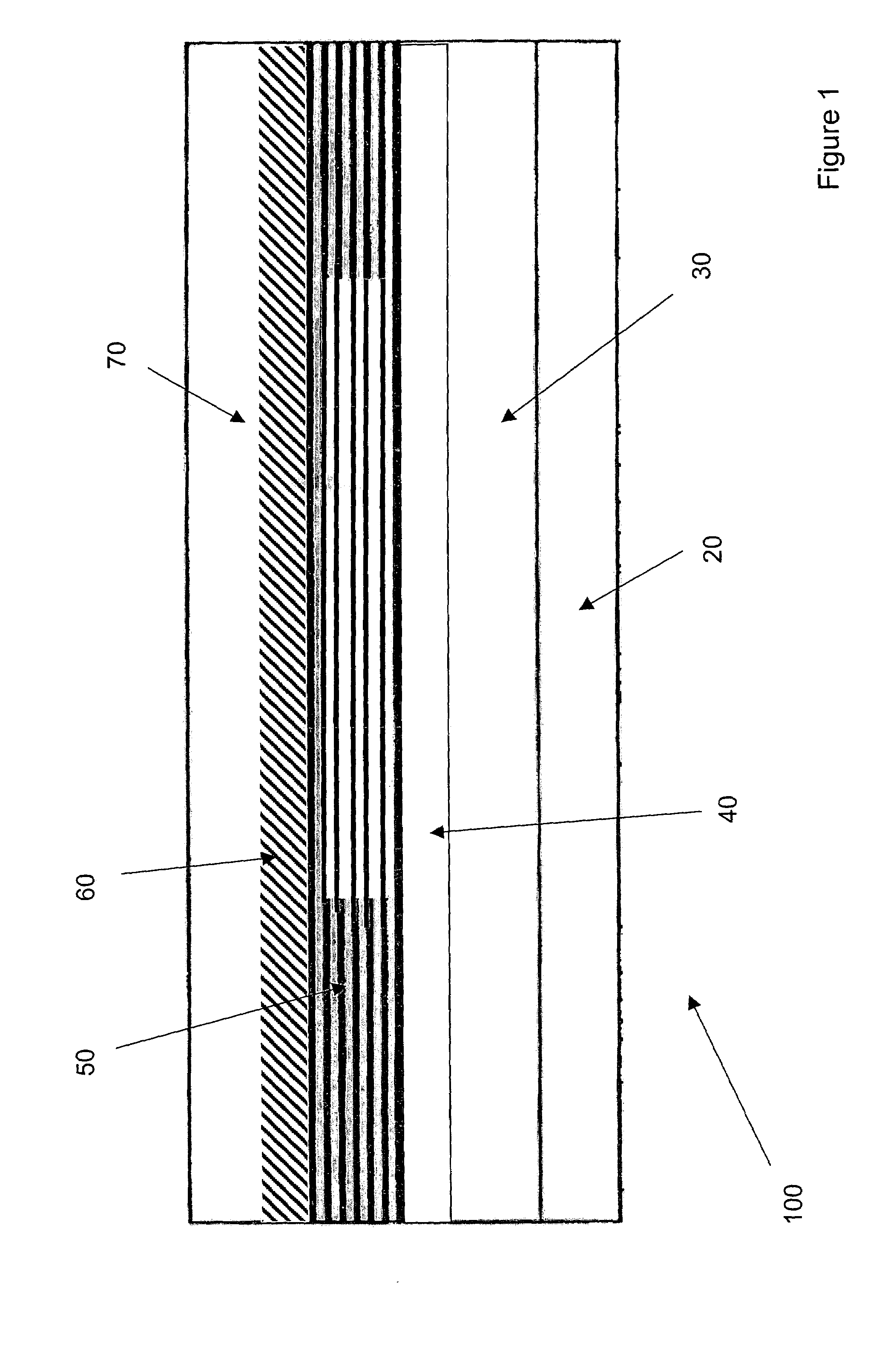
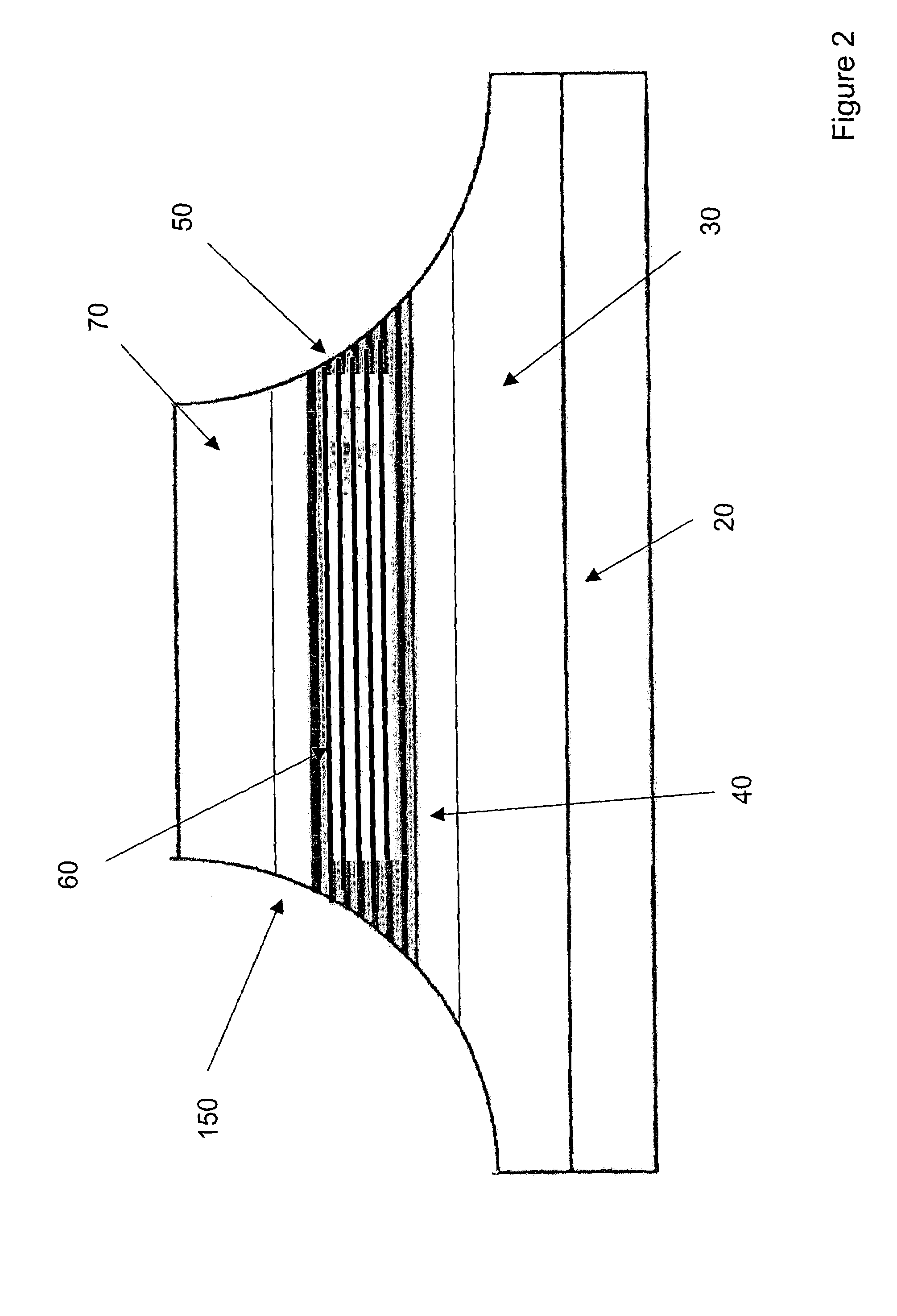
[0018]FIG. 1 shows a schematic depiction of a wafer 100 from which a semiconductor device according to the present invention can be fabricated. The wafer 100 comprises an InP substrate 20 that is doped with an n-type dopant (with a doping density of approximately 4×1018 cm−3). A plurality of layers are formed on top of the substrate 20: lower cladding layer 30 comprises n-type InP with a thickness of about 1.5 μm and a doping density of approximately 2.5×1018 cm−3; an undoped first confinement layer 40 comprising InGaAsP lattice matched to InP; multiple quantum well structure 50 comprising undoped strained InGaAsP; second confinement layer 60 comprising undoped InGaAsP lattice matched to InP; and second cladding layer 70 comprising p-type InP with a thickness of about 0.4 μm and a doping density of approximately 1.5×1018 cm−3.

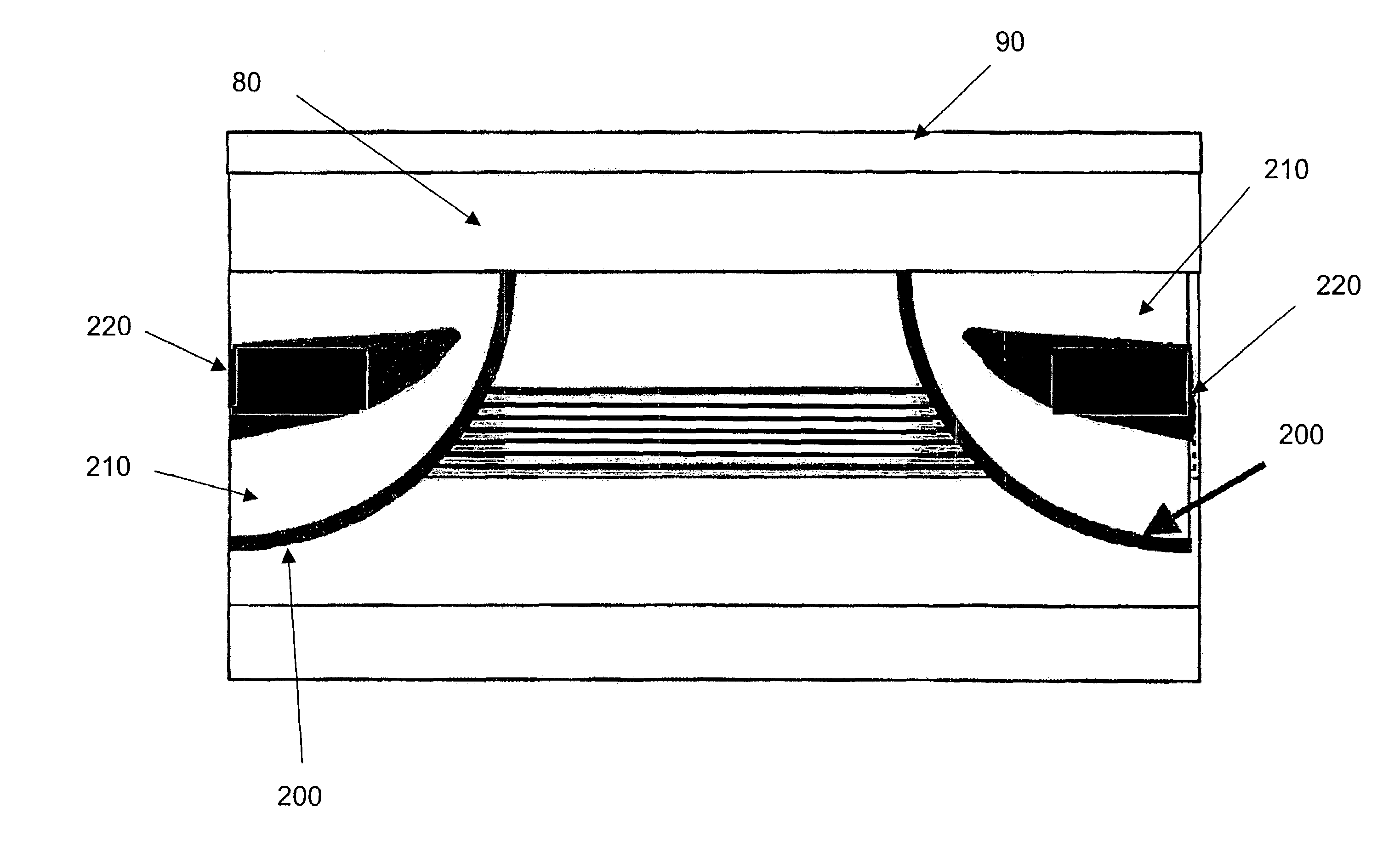
[0019]Once the wafer has been fabricated as described above with reference to FIG. 1, a laser stripe will be defined by photolithographically depositing an oxi...


PUM


Abstract

A semiconductor device is disclosed in which a barrier layer is deposited on the sides of the mesa. The barrier layer may comprise a semiconductor material. The barrier layer reduces diffusion of dopants into the active region of the device.

Description

FIELD OF THE INVENTION[0001]The present invention relates to semiconductor devices and in particular to the processing of buried heterostructures to mitigate the unwanted diffusion of dopant atoms into the active region of a semiconductor device.DISCUSSION OF THE BACKGROUND ART[0002]Buried heterostructures (BHs) are used in a number of semiconductor devices, for example distributed feedback and Fabry-Perot lasers. A buried heterostructure is formed by etching a semiconductor wafer to form a mesa and then depositing overgrowth layers of semiconductor material around the sides of the mesa. Suitable selection of the materials and the doping of the overgrowth layers provide the desired performance of the device. It has been observed that the dopants from the overgrowth layers have a tendency to become deactivated from the overgrowth layers and then to diffuse out of the overgrowth layers. If some of these dopant atoms diffuse into the active region of the semiconductor device then the p...

Claims


Application Information

Patent Timeline
Patent Type & Authority Patents(United States)
IPC IPC(8): H01L33/00H01L29/06H01S5/00H01S5/22H01S5/227
CPCH01S5/227H01S5/2209H01S5/2226H01S5/2275
Inventor MASSA, JOHN STEPHENWOOD, SIMON ANDREW
Owner BROADCOM INT PTE LTD
Why Eureka
Try Eureka