

Radiation-emitting chip
a technology of radiation-emitting chips and semiconductors, applied in the direction of semiconductor/solid-state device manufacturing, electrical apparatus, semiconductor devices, etc., can solve the problems of component failure and the location of the pn junction
Inactive Publication Date: 2005-05-24
OSRAM OLED
View PDF23 Cites 32 Cited by
- Summary
- Abstract
- Description
- Claims
- Application Information
AI Technical Summary
Benefits of technology
[0005]One object of the invention is to provide an improved radiation-emitting chip of the type described above in which, in particular, the risk of a short circuit of the active region or a part of the active region is eliminated to the greatest possible extent.
[0008]In the case of the chip according to an embodiment of the invention, the photon-emitting active region is far enough away from any electrically conductive connecting means for fixing the chip on a chip carrier, so that the risk of an electrical short circuit of the active region by the electrically conductive connecting means is eliminated to the greatest possible extent. The chip according to the invention can therefore be mounted reliably.
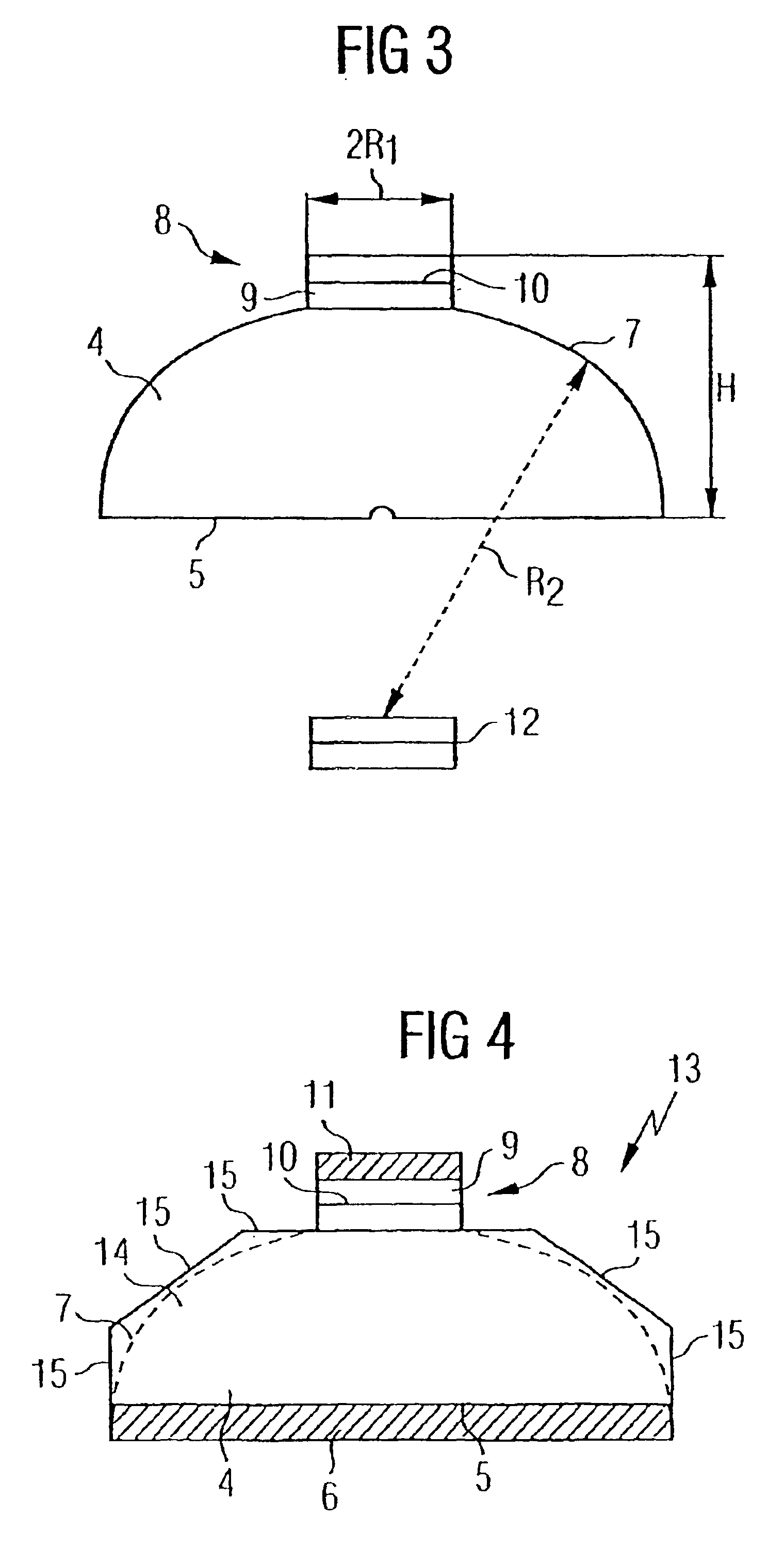
[0012]The invention is particularly preferably suitable for chips in which the material of the coupling-out window has a larger refractive index than the material of the active region which adjoins the latter, said active region usually being formed as an active multilayer structure. As a result, the reflection of the radiation emitted by the active zone toward the rear at the interface between active region and coupling-out window is advantageously reduced and the radiation coupled into the coupling-out window is compressed.
Problems solved by technology
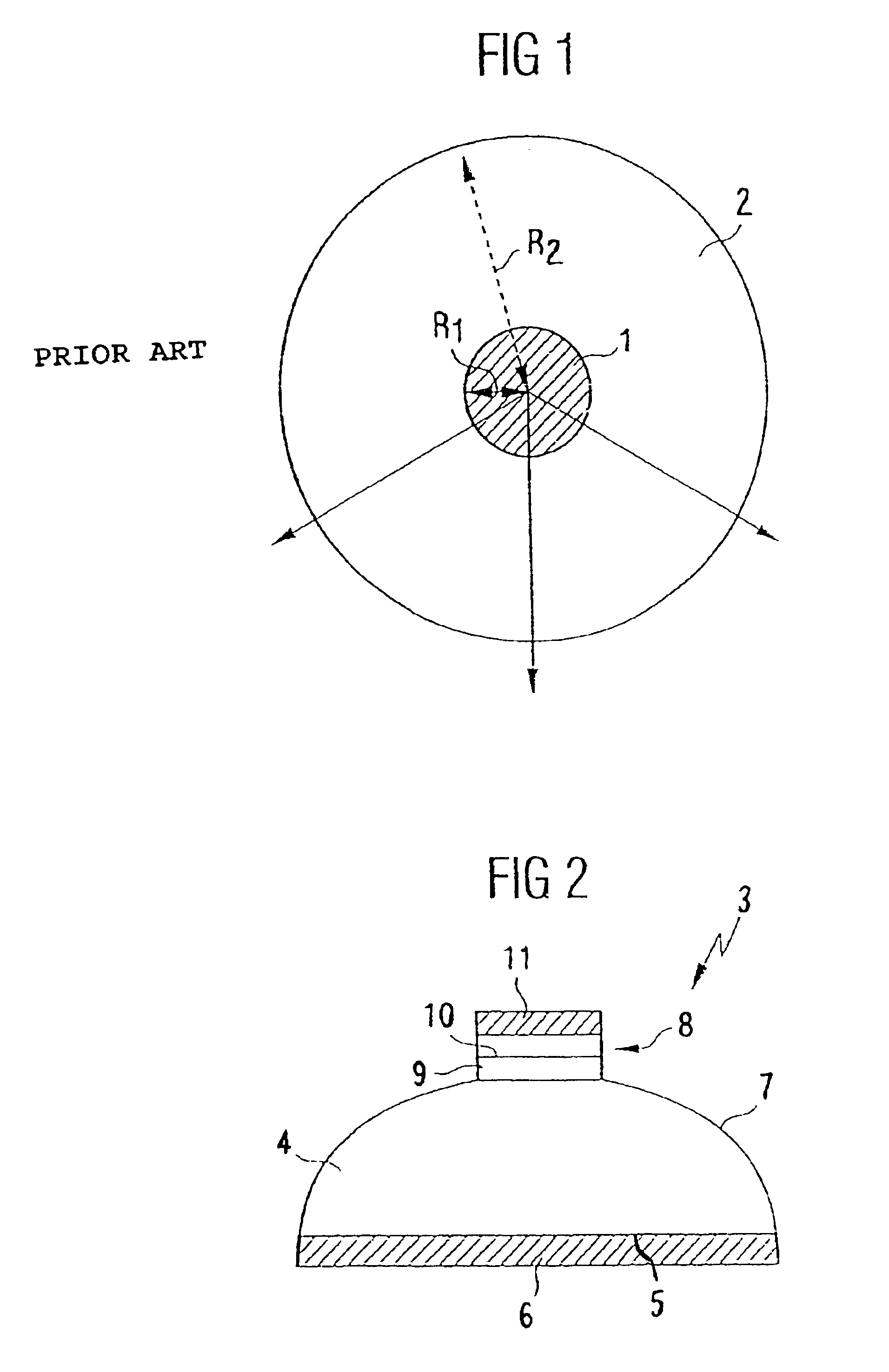
One disadvantage of the known light-emitting diode chip is that the pn junction is situated at the mounting side of the chip.
In the case of mounting using electrically conductive silver-epoxy adhesive, there is therefore a high risk that adhesive swelling up laterally will electrically short-circuit the active region, leading to the failure of the component.
Method used
View moreImage
Smart ImageViewing Examples

Examples
example 2
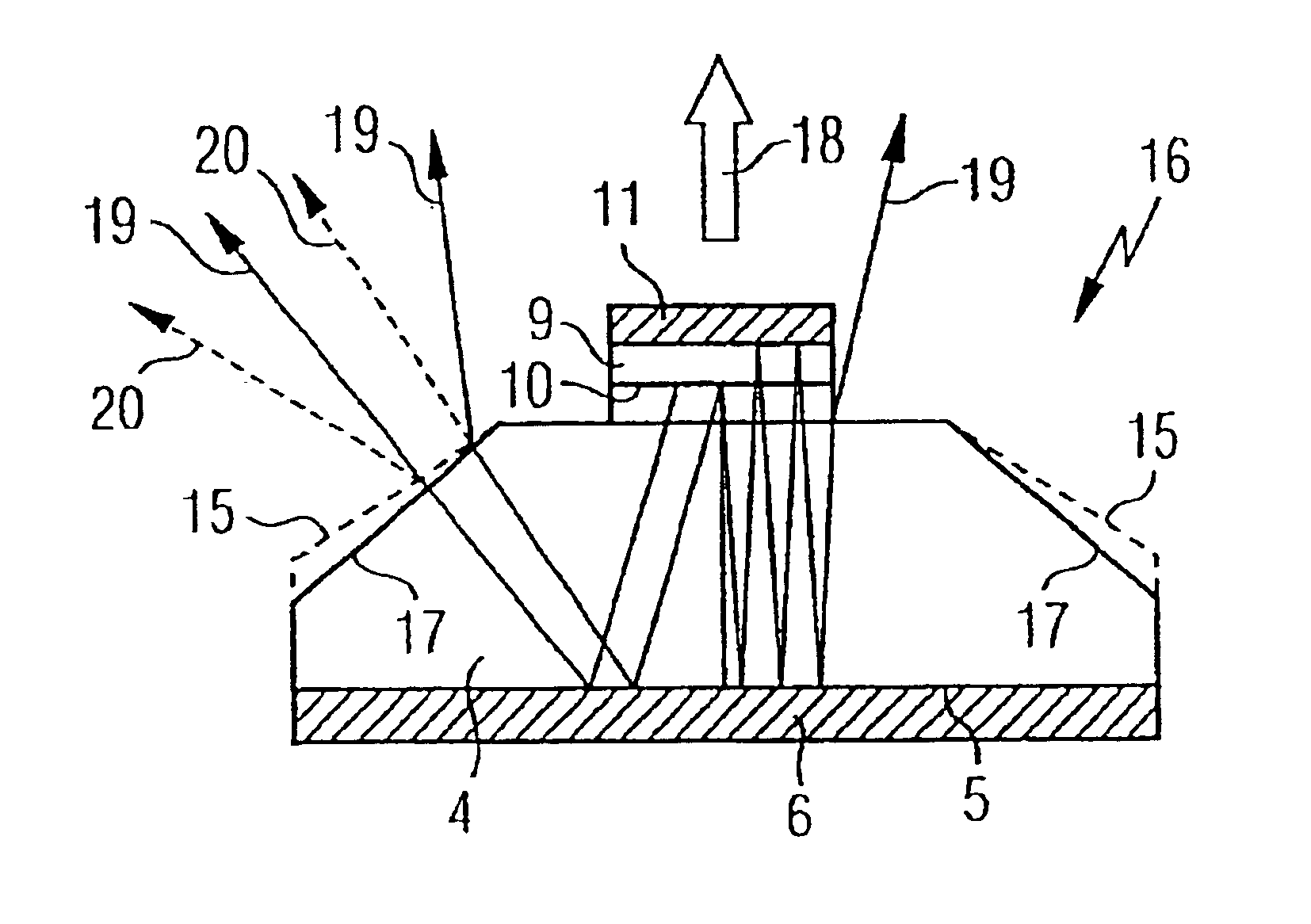
[0045]In a further chip 16, which differs from the chip 16 from example 1 only by an angle of inclination of the side areas 17 of 45 degrees, the coupling-out efficiency was 39%.
Login to View More PUM
 Abstract
A light-emitting chip (3) has a lens-type coupling-out window (4), whose base area (5) is provided with a mirror area (6). Arranged on a coupling-out area (7) of the coupling-out window (4) is a layer sequence (9), with a photon-emitting pn junction (10). The photons emitted by the pn junction are reflected at the mirror area (6) and can leave the coupling-out window (4) through the coupling-out area (7).
Description
[0001]This is a U.S. national stage of application Ser. No. DE01 / 04171, filed on 06 Nov. 2001.FIELD OF THE INVENTION[0002]The invention relates to a radiation-emitting chip having a photon-emitting active region and a coupling-out window which is assigned to the latter, in particular adjoins the latter, and has a coupling-out area via which at least a part of the radiation emitted by the active region is coupled out from the chip.[0003]U.S. Pat. No. 5,087,949 A discloses a light-emitting diode chip having an n-doped coupling-out window in the shape of a truncated pyramid. A p-conducting layer is formed along the base area of the n-conducting base body. An insulating layer interrupted by a central window is situated below the p-conducting layer. In the window, the p-conducting layer is contact-connected by a contact layer. A further contact layer is situated on the top side of the base body in the shape of a truncated pyramid. Through the insulating layer, the current flow through th...
Claims
Login to View More Application Information
Patent Timeline
 Patent Type & AuthorityPatents(United States)
IPC IPC(8): H01L33/00H01L33/02H01L33/08H01L33/20H01L33/40
CPCH01L33/02H01L33/20H01L33/405H01L33/08
InventorBAUR, JOHANNESEISERT, DOMINIKFEHRER, MICHAELHAHN, BERTHOLDHARLE, VOLKERJACOB, ULRICHOBERSCHMID, RAIMUNDPLASS, WERNERSTRAUSS, UWEVOLKL, JOHANNESZEHNDER, ULRICH
OwnerOSRAM OLED