Method of growing a thin film onto a substrate

a technology of thin film and substrate, which is applied in the direction of crystal growth process, chemically reactive gas, pressurized chemical process, etc., can solve the problems of reducing the risk of microparticle formation already in the infeed line, affecting generally having a deteriorating effect on the quality of the deposited thin film, so as to reduce the risk of particles and droplets absorbed in the purifier being released therefrom, the risk of investment cost and the need of maintenan

Inactive Publication Date: 2004-12-30
ASM IP HLDG BV
View PDF4 Cites 180 Cited by
  • Summary
  • Abstract
  • Description
  • Claims
  • Application Information

AI Technical Summary

Benefits of technology

[0004] In the MBE and CVD processes, besides other variables, the thin film growth rate is also affected by the concentrations of the provided starting material inflows. To achieve a uniform surface smoothness of the thin films manufactured using these methods, the concentrations and reactivities of the starting materials must be kept equal over the whole surface area of the substrate. If the different starting materials are allowed to mix which each other prior to reaching the substrate surface, as is the case in the CVD method, the possibility of mutual reactions between the reagents is always imminent. Herein arises a risk of microparticle formation already in the infeed lines of the gaseous reactants. Such microparticles generally have a deteriorating effect on the quality of the deposited thin film. However, the occurrence of premature reactions in MBE and CVD reactors can be avoided, e.g., by heating the reactants not earlier than only at the substrates. In addition to heating, the desired reaction can be initiated with the help of e.g., plasma or other similar activating means.
[0008] According to the conventional techniques known from FI Patent Specification No. 57,975, the saturation step is followed by a protective gas pulse forming a diffusion barrier that sweeps away the excess starting material and the gaseous reaction products from the substrate. Intermixing of the successive reactant pulses must be avoided. The successive pulses of different starting materials and the protective gas pulses forming diffusion barriers that separate the successive starting materials pulses from each other accomplish the growth of the thin film at a rate controlled by the surface chemistry properties of the different materials.
[0010] An essential feature of the ALD process is that condensation of the reactant should be avoided in the vicinity of the reaction chamber. Condensation of the reactant in particular in the conduit between the reactant source and the reaction chamber and on the substrate in the reaction chamber will seriously impair the quality of the thin film. Particles or droplets condensed or sublimed in the reactant feed lines may disperse into the reactant flow and cause inhomogenity on the thin film. The same applies to condensation of solid particles or liquid droplets on the thin film in the reaction chamber. Therefore, an ALD process is operated in such a manner that the temperature in the equipment interconnecting the reactant source and the outlet of the reaction chamber (the "hot zone") is not allowed to drop below the condensation temperature of the reactant.
[0014] It is an object of the present invention to provide a novel method of growing a thin film onto a substrate placed in a reaction chamber according to the ALD process. In particular, it is an object of the invention to provide a method in which the ALD process can be operated using solid or liquid reactant sources and employing a purifier for removing solid particles or liquid droplets emanating from, e.g. the precursor sources, while minimizing the costs and the wear of the process equipment.
[0018] Considerable advantages are obtained by means of the invention. Thus, by means of the present process moving mechanical parts can be avoided in all or most of the area operated at a temperature above the evaporation temperature. The operation of the present regulating mechanism, in the following also called "inert gas valving" is reliable and it is not sensitive to variations in the chemical character of the precursors. Since it includes no moving parts, the investment costs and the need for maintenance work is strongly reduced. As will be discussed in more detail below, by the inert gas valving system, pulsing of reactants can be carried out by using only one valve which controls the flow of carrier gas from the source of inactive or inert gas to the precursor source. This valve can be kept at ambient temperature and it is not in direct contact with the reactants. By maintaining the temperature of the draining conduit above the evaporation temperature of the reactant, condensation of the reactant in the hot zone of the apparatus can be avoided. There is no build-up of condensated reactants in the third conduit during the purse phase. All parts of the equipment are kept cleaner and there are formed less particles which could be forwarded to the reaction chamber. Precursor waste during the purge cycle can be minimized by providing for static gas flow conditions in the source.
[0019] According to a preferred embodiment, wherein the purifier is incorporated into the conduit interconnecting the reactant source with the reaction chamber, the inert gas barrier is arranged downstream of the purifier whereby there is a one-way flow of gas over the purifier during the whole operation of the ALD process. Since the flow direction over and through the purifier does not change, the risk of particles and droplets absorbed in the purifier being released therefrom is eliminated.

Problems solved by technology

Herein arises a risk of microparticle formation already in the infeed lines of the gaseous reactants.
Such microparticles generally have a deteriorating effect on the quality of the deposited thin film.
Condensation of the reactant in particular in the conduit between the reactant source and the reaction chamber and on the substrate in the reaction chamber will seriously impair the quality of the thin film.
Particles or droplets condensed or sublimed in the reactant feed lines may disperse into the reactant flow and cause inhomogenity on the thin film.
Therefore, an ALD process is operated in such a manner that the temperature in the equipment interconnecting the reactant source and the outlet of the reaction chamber (the "hot zone") is not allowed to drop below the condensation temperature of the reactant.
When solid reactant sources are used, a carrier gas typically has to be employed for feeding the reactant vapours into the reaction chamber because the vapour pressure of the source is not always sufficient to allow for a sufficiently strong flow of vapour-phase reactant pulses from the source to the reaction chamber.
Since many of the solid sources are powders containing extremely finely divided matter (dust), there is a risk for contamination of the vapour-phase reactant pulses with small solid particles when the carrier gas flow is conducted through the reactant material.
These particles disturb the growth of the thin film.
Similar problems are encountered with liquid reactants having high boiling points in that the flow of the carrier gas may create a mist with finely divided droplet dispersed in the carrier gas flow.
These conditions are particularly demanding for mechanical valves conventionally employed for, e.g., pulsing of the reactants and purge gas, and for the gaskets and packings of said valves and other fittings.
Attrition of the polymer materials used in the gaskets and packings will cause an additional dusting problem resulting in contamination of the vapour-phase reactant pulses.

Method used


Image

  • Method of growing a thin film onto a substrate
  • Method of growing a thin film onto a substrate
  • Method of growing a thin film onto a substrate

Examples


Embodiment Construction

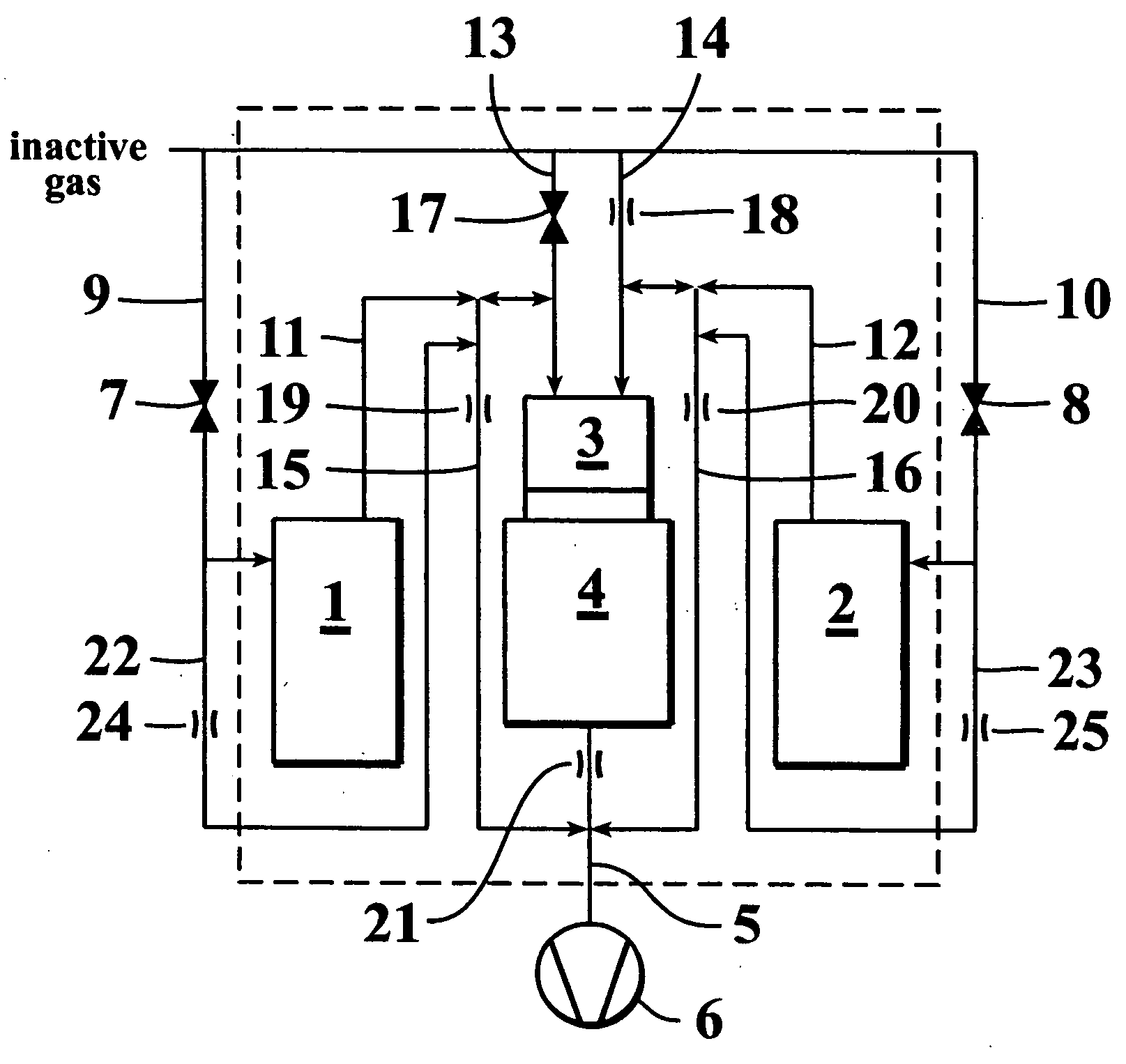
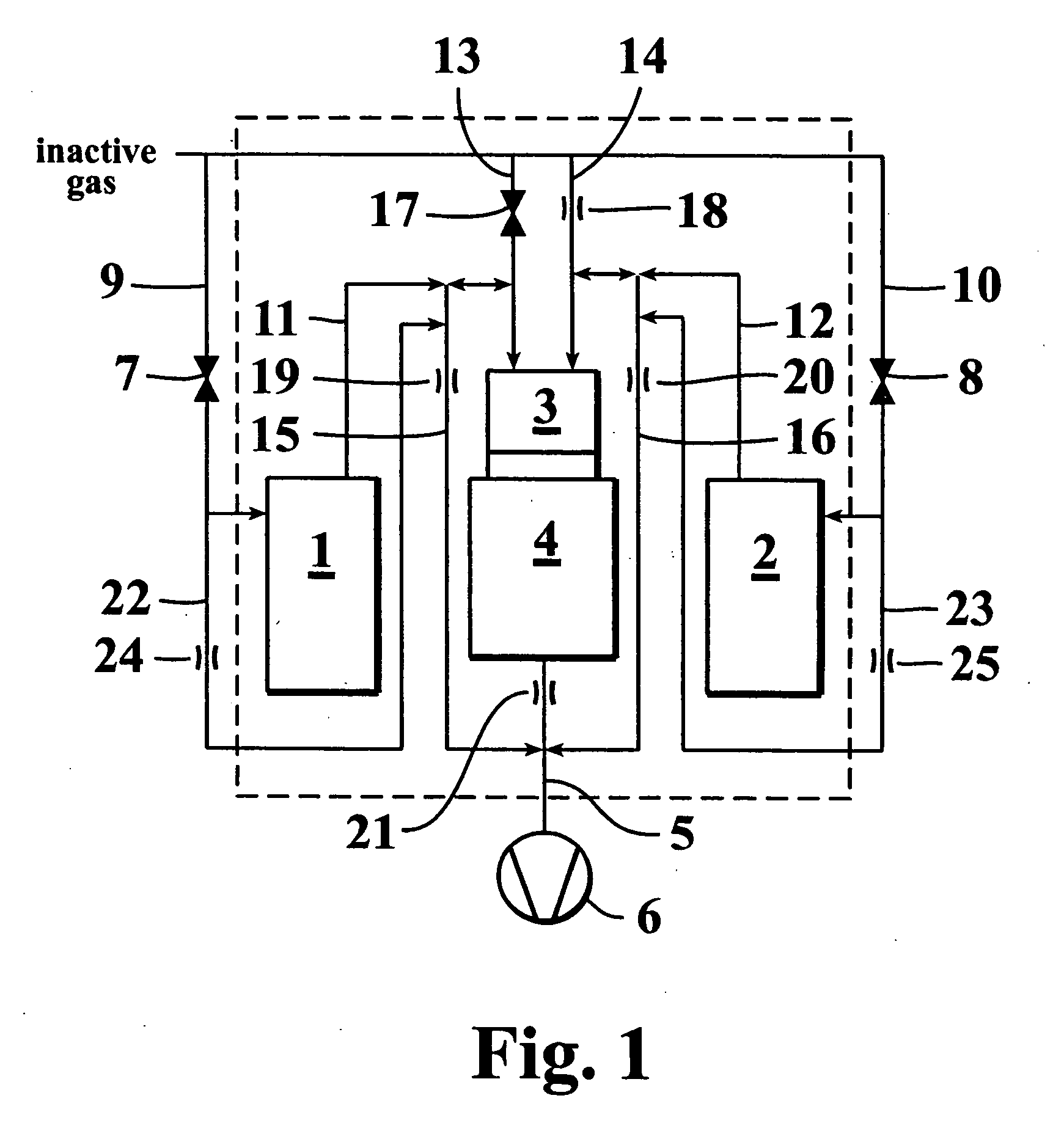
[0059] A process configuration according to the present invention was tested by building an ALD processing unit using pipes having a diameter of 1 / 4 inches (about 6 mm) and comprising conduits

[0060] 1) for connecting the reactant source with the reactor (the "first conduit"),

[0061] 2) for introducing inactive gas into the connection pipe (the "second conduit") and

[0062] 3) for withdrawing inactive gas from the connection pipe (the "third conduit").

[0063] The third conduit was connected to the first conduit at a distance of about 10 cm from the connection point of the second conduit. In the following, the portion of the first conduit extending between these two connection point is called the "barrier zone" or "barrier portion." A porous filter layer was incorporated into the first conduit between the reactant source and the connection point of the third conduit. The reactant sources tested comprised various solid and liquid precursors which were conducted with a carrier gas from the ...


PUM

PropertyMeasurementUnit
temperatureaaaaaaaaaa
pressureaaaaaaaaaa
pressureaaaaaaaaaa

Abstract

A method of growing a thin film onto a substrate placed in a reaction chamber according to the ALD method by subjecting the substrate to alternate and successive surface reactions. The method includes providing a first reactant source and providing an inactive gas source. A first reactant is fed from the first reactant source in the form of repeated alternating pulses to a reaction chamber via a first conduit. The first reactant is allowed to react with the surface of the substrate in the reaction chamber. Inactive gas is fed from the inactive gas source into the first conduit via a second conduit that is connected to the first conduit at a first connection point so as to create a gas phase barrier between the repeated alternating pulses of the first reactant entering the reaction chamber. The inactive gas is withdrawn from said first conduit via a third conduit connected to the first conduit at a second connection point.

Description

PRIORITY INFORMATION[0001] This application claims the priority benefit under 35 U.S.C. .sctn.119 to Finnish Patent Application No. 20000900, filed Apr. 14, 2000, the entire content of which is hereby expressly incorporated by reference.[0002] The present invention relates to growing thin films on a surface of a substrate. More particularly, the invention concerns an improved method and apparatus for producing a thin film onto a substrate by subjecting the substrate to alternately repeated surface reactions of vapor-phase reactants.DESCRIPTION OF THE RELATED ART AND SUMMARY OF THE INVENTION[0003] Conventionally, thin films are grown out using a vacuum evaporation deposition. Molecular Beam Epitaxy (MBE) and other similar vacuum deposition techniques, different variants of Chemical Vapor Deposition (CVD) (including low-pressure and metallo-organic CVD and plasma-enhanced CVD) or, alternatively, the above-mentioned deposition process based on alternate surface reactions, known in the ...

Claims


Application Information

Patent Timeline
Patent Type & Authority Applications(United States)
IPC IPC(8): B03C3/28B01J3/00B01J3/02B01J19/00C23C16/44C23C16/455C30B25/14H01L21/205
CPCC23C16/4402C23C16/4482C23C16/45527Y10T117/1008C23C16/45561C30B25/14Y10T117/1004C23C16/45544H01L21/20
Inventor LINDFORS, SVENSOININEN, PEKKA T.
Owner ASM IP HLDG BV
Why Eureka
Try Eureka