Strained channel FinFET

a finfet and channel technology, applied in the field of transistors, can solve the problems of difficult, if not impossible, scaling of existing bulk mosfet devices below 0.1 m process generation, etc., and achieve the effect of increasing the drive current of the finfet transistor, increasing the carrier mobility, and increasing the carrier mobility

Inactive Publication Date: 2005-05-24
INNOVATIVE FOUNDRY TECH LLC
View PDF7 Cites 117 Cited by
  • Summary
  • Abstract
  • Description
  • Claims
  • Application Information

AI Technical Summary

Benefits of technology

[0005]Consistent with the present invention, a FinFET transistor is provided that uses a vertically formed strained channel layer that is self-aligned to the fin channel. The strained channel layer may include a crystalline material that is lattice constant mismatched with the crystallin

Problems solved by technology

Due to limitations associated with existing gate-oxide thicknesses and source/drain (S/D) junction depths, sc

Method used


Image

  • Strained channel FinFET
  • Strained channel FinFET
  • Strained channel FinFET

Examples


Embodiment Construction

[0021]The following detailed description of the invention refers to the accompanying drawings. The same reference numbers in different drawings may identify the same or similar elements. Also, the following detailed description does not limit the invention. Instead, the scope of the invention is defined by the appended claims.

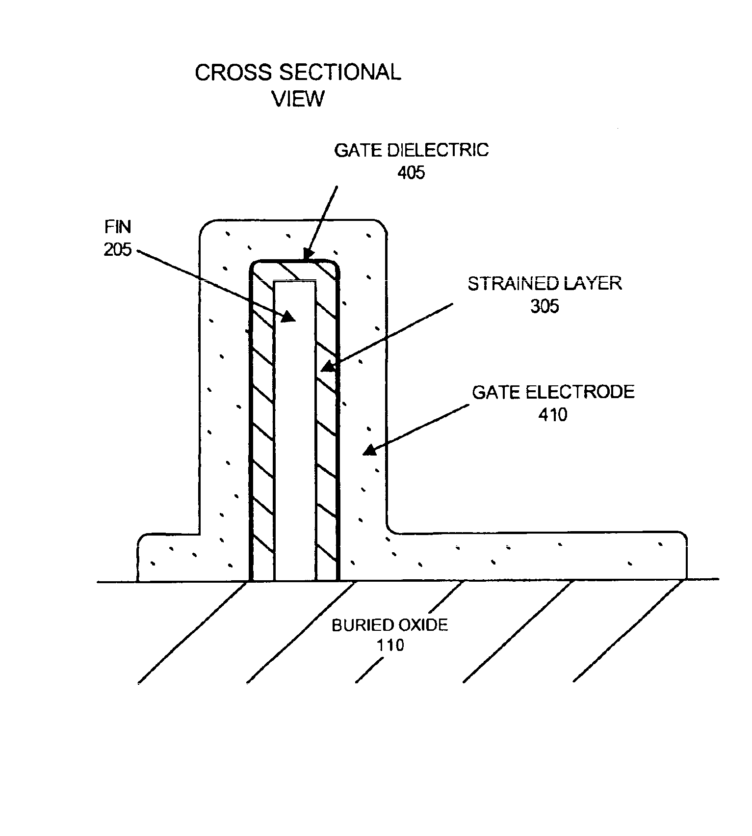
[0022]Consistent with the present invention, an increased mobility channel FinFET is provided. A vertically formed strained channel layer, consistent with the present invention, is self-aligned to the fin channel of the FinFET. The strained channel layer may include a crystalline material that is lattice mismatched with the crystalline material of the fin of the FinFET such that tensile strain is induced within the strained channel layer. The induced tensile strain increases carrier mobility of the strained channel layer, thus, increasing drive current of the FinFET.

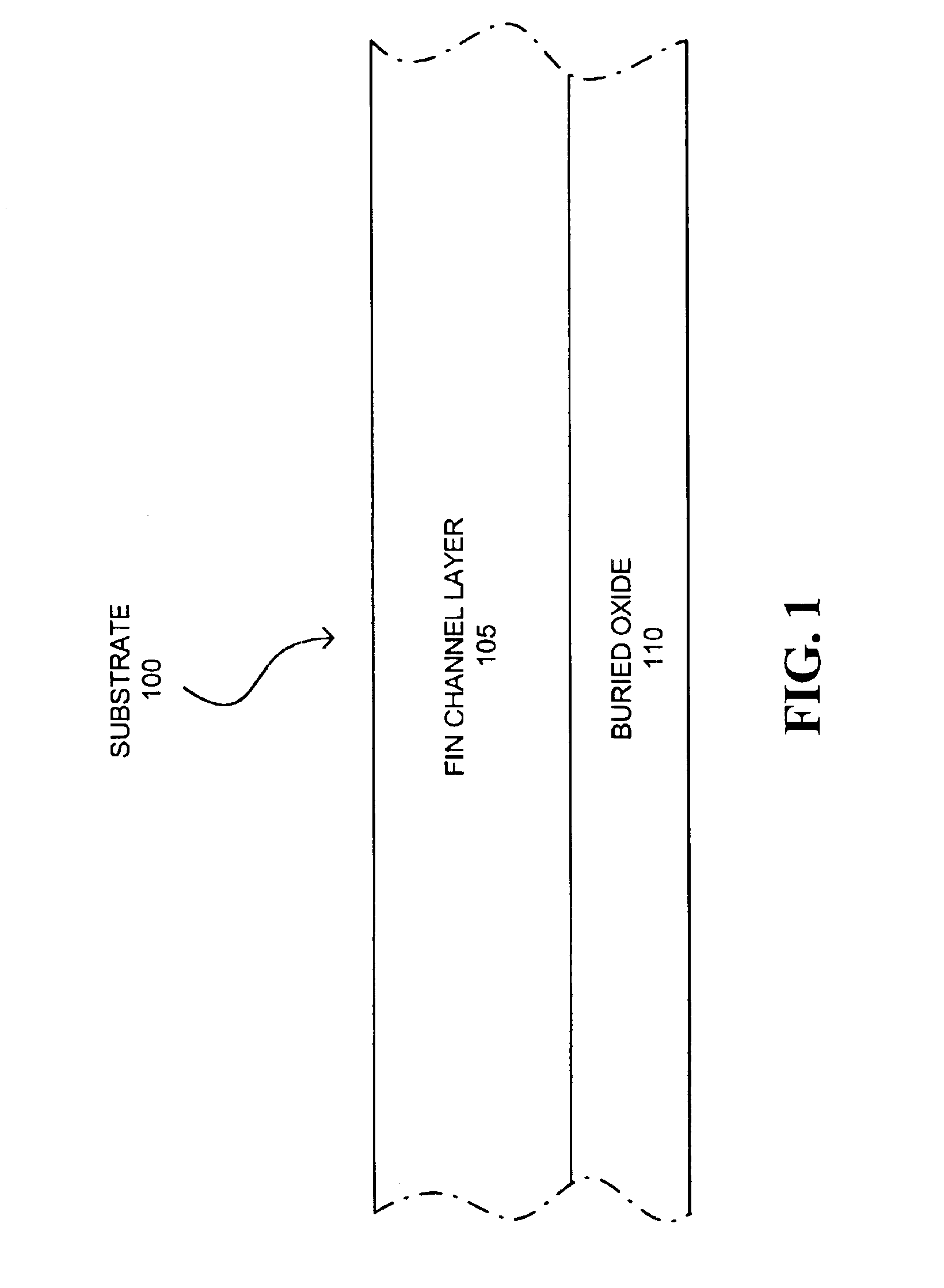
[0023]FIG. 1 illustrates a cross-section of a substrate 100 formed in accordance with an exempla...


PUM


Abstract

A semiconductor device includes a fin and a layer formed on at least a portion of the fin. The fin includes a first crystalline material. The layer includes a second crystalline material, where the first crystalline material has a larger lattice constant than the second crystalline material to induce tensile strain within the layer.

Description

RELATED APPLICATION[0001]This application is a continuation of U.S. Ser. No. 10 / 349,042, filed on Jan. 23, 2003, now U.S. Pat. No. 6,803,631 the disclosure of which is hereby incorporated herein by reference.TECHNICAL FIELD[0002]The present invention relates generally to transistors and, more particularly, to fin field effect transistors (FinFETs).BACKGROUND ART[0003]Scaling of device dimensions has been a primary factor driving improvements in integrated circuit performance and reduction in integrated circuit cost. Due to limitations associated with existing gate-oxide thicknesses and source / drain (S / D) junction depths, scaling of existing bulk MOSFET devices below the 0.1 μm process generation may be difficult, if not impossible. New device structures and new materials, thus, are likely to be needed to improve FET performance.[0004]Double-gate MOSFETs represent new devices that are candidates for succeeding existing planar MOSFETs. In double-gate MOSFETs, the use of two gates to c...

Claims


Application Information

Patent Timeline
IPC IPC(8): H01L21/02H01L21/336H01L29/10H01L29/66H01L29/02H01L29/786H01L29/49H01L29/40
CPCH01L29/1054H01L29/78687H01L29/785H01L29/78654H01L29/66795H01L29/4908
Inventor DAKSHINA-MURTHY, SRIKANTESWARAAN, JUDY XILINKRIVOKAPIC, ZORANWANG, HAIHONGYU, BIN
Owner INNOVATIVE FOUNDRY TECH LLC
Why Eureka
Try Eureka