Semiconductor device and method of manufacturing same

Inactive Publication Date: 2005-05-24
RENESAS TECH CORP
View PDF3 Cites 54 Cited by
  • Summary
  • Abstract
  • Description
  • Claims
  • Application Information

AI Technical Summary

Benefits of technology

[0033]The semiconductor device according to the present invention, which has the foregoin

Problems solved by technology

However, the above-mentioned prior art examples do no

Method used


Image

  • Semiconductor device and method of manufacturing same
  • Semiconductor device and method of manufacturing same
  • Semiconductor device and method of manufacturing same

Examples


Example

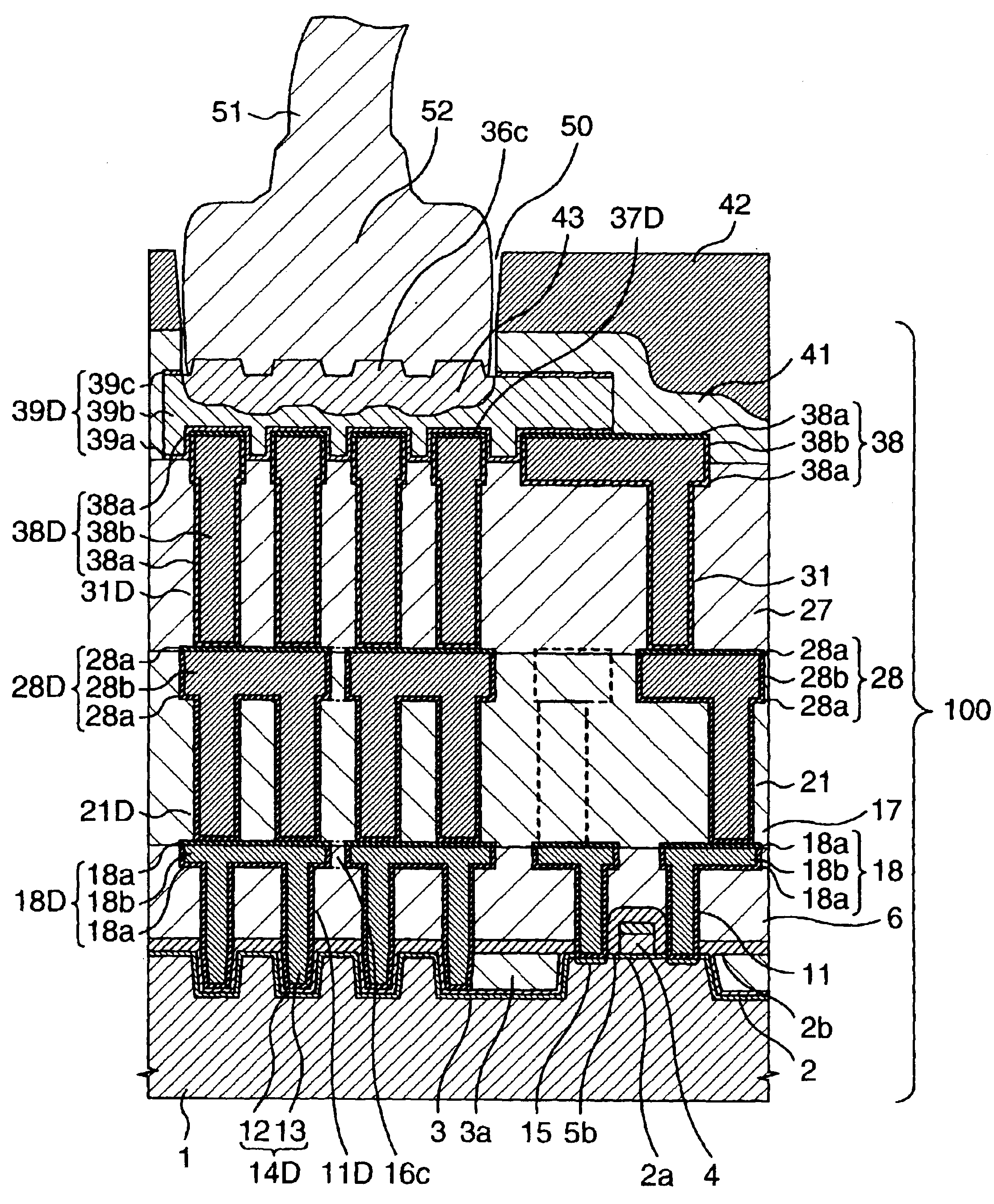
[0043]A semiconductor device according to one embodiment of the present invention is illustrated in FIG. 1. FIG. 1 is a cross-sectional view schematically illustrating the semiconductor device 100 according to this embodiment, which is applied to a processing unit, by way of example. A pad structure is illustrated in a left-hand region of the drawing, while the structure of a processing circuit is illustrated in a right-hand region.

[0044]The semiconductor chip 100 in FIG. 1 comprises a shallow groove feature 3 formed on a silicon substrate 1 for separating elements; and plugs 14D, a first dummy wiring layer 16D, plugs 24D, a second wiring layer 26, plugs 34D, and a third wiring layer 36 which are laminated on the shallow groove feature 3. The third wiring layer 36 additionally serves as a pad. The plugs 34D protrude into the pad 36 by 30 nanometers or more to improve the bonding strength between the pad 36 and an underlying interlayer insulating film 27. While FIG. 1 shows that the ...


PUM


Abstract

A highly reliable semiconductor device provided herein can prevent a junction between a pad and a wire from coming off, and pads from peeling off an underlying insulating layer on the interface thereof. The semiconductor device has plugs formed in a region in which an electrode pad is formed over a substrate. The plugs protrude into the electrode pad.

Description

BACKGROUND OF THE INVENTION[0001]The present invention relates to a semiconductor device, and more particularly, to a semiconductor device which has pads formed on the surface thereof for electric communications to the outside. The present invention also relates to a method of manufacturing the semiconductor device.[0002]The primary importance to the development of large capacity semiconductor devices includes a lower cost and faster operations of the devices through a reduction in chip sizes. Further, in semiconductor devices intended for providing higher performance and more functions, bonding pads (hereinafter simply called the “pads”) for electrical connections of a chip to the outside must be formed at a narrower pitch in order to simultaneously increase the number of input / output terminals and reduce the chip size. When 240 pads are formed, for example, along four sides of a chip in the shape of a 5-mm square, each pad must be reduced in width to 70 micrometers or less when th...

Claims


Application Information

Patent Timeline
IPC IPC(8): H01L23/52H01L23/522H01L23/485H01L23/48H01L21/60
CPCH01L23/5226H01L24/03H01L24/05H01L24/48H01L24/45H01L2224/04042H01L2224/05082H01L2224/05093H01L2224/05096H01L2224/05166H01L2224/05187H01L2224/05556H01L2224/05557H01L2224/05558H01L2224/05624H01L2224/45015H01L2224/45144H01L2224/4807H01L2224/48463H01L2224/48624H01L2224/85205H01L2924/01002H01L2924/01004H01L2924/01006H01L2924/01013H01L2924/01014H01L2924/01022H01L2924/01025H01L2924/01027H01L2924/01029H01L2924/0105H01L2924/01074H01L2924/01078H01L2924/01079H01L2924/01082H01L2924/014H01L2924/04941H01L2924/05042H01L2924/20106H01L2924/20303H01L2924/20752H01L2924/30105H01L2924/01033H01L2924/01044H01L2224/45147H01L2224/48453H01L2224/48799H01L2224/02166H01L2924/00014H01L2924/04953H01L2924/00H01L23/485H01L2224/45124H01L2224/48724H01L2224/48824
Inventor NAKAJIMA, TAKASHITANAKA, NAOTAKANAKAJIMA, YASUYUKIHARUTA, RYOMATSUZAWA, TOMOOSAHARA, MASASHIOKUTANI, KEN
Owner RENESAS TECH CORP
Why Eureka
Try Eureka