Programmable logic array integrated circuits

a logic array and integrated circuit technology, applied in the direction of instruments, computation using denominational number representation, pulse technique, etc., can solve the problems of increasing the complexity of the logic which can be performed, increasing the complexity of the task of programming the circuit,

Inactive Publication Date: 2005-05-24
ALTERA CORP
View PDF65 Cites 41 Cited by
  • Summary
  • Abstract
  • Description
  • Claims
  • Application Information

AI Technical Summary

Benefits of technology

[0019]Another interconnection technique which can be advantageously employed in accordance with the principles of this invention is to group the programmable logic elements into a plurality of mutually exclusive groups, each group having associated with it one or more conductors which can only be used to interconnect the elements in that group. In addition, there are other conductors which can be used to convey signals between the groups. Grouping the programmable logic elements in mutually exclusive (i.e., non-overlapping) groups helps to simplify the task of programming the device by breaking the device down into several discrete parts, each of which is smaller and more easily managed than the whole device. Providing signal conductors which serve only to interconnect the programmable logic elements in each group avoids tying up much longer conductors just to make short interconnections between adjacent programmable logic elements. This helps to reduce the required number of long conductors.
[0021]Multiplexers can also be used in combination with programmable signal conductor interconnections to allow certain of the conductors to be laid down more densely, to reduce the size of the interconnection array, and to reduce the capacitive loading on each output conductor of the array. Instead of one output conductor crossing a large number of parallel input conductors with a programmable interconnection at each intersection of the output conductor with the input conductors (which tends to force relatively wide spacing of the input conductors because of the relatively large size of the programmable interconnections), two substantially parallel output conductors feeding a programmably controlled output multiplexer are used. Each of these output conductors has a programmable interconnection only with every other one of the input conductors, and the input conductors which are thus connectable to one of the output conductors are interdigitated with the input conductors which are connectable to the other one of the output conductors. By thus spreading the programmable interconnections somewhat parallel to the longitudinal axes of the input conductors, the input conductors can be placed more closely together, which may save valuable space on the integrated circuit. This technique can also be used and further enhanced to reduce the number of programmable elements required to control the programmable interconnections between the input and output conductors if desired. In particular, a single programmable element can be used to control two interconnections, one of which is on one output conductor, and the other of which is on the other output conductor. The output multiplexer then makes the final selection of the desired output signal. Reducing the number of programmable elements in this way may be especially beneficial when the programmable elements are relatively large (e.g., as compared to the signal conductor interconnection elements they control). Indeed, it may be desirable to use more than two output signal conductors feeding the programmably controlled output multiplexer and to have each programmable element control one interconnection element on each of the more than two output conductors to still further reduce the required number of programmable elements.

Problems solved by technology

Similarly, as the number of programmable elements increases, the complexity of the logic which can be performed also increases.
But this in turn tends to increase the complexity of the task of programming the circuit unless additional logical structure is included in the circuit to help correspondingly structure the programming task.

Method used


Image

  • Programmable logic array integrated circuits
  • Programmable logic array integrated circuits
  • Programmable logic array integrated circuits

Examples


first embodiment

I. First Embodiment

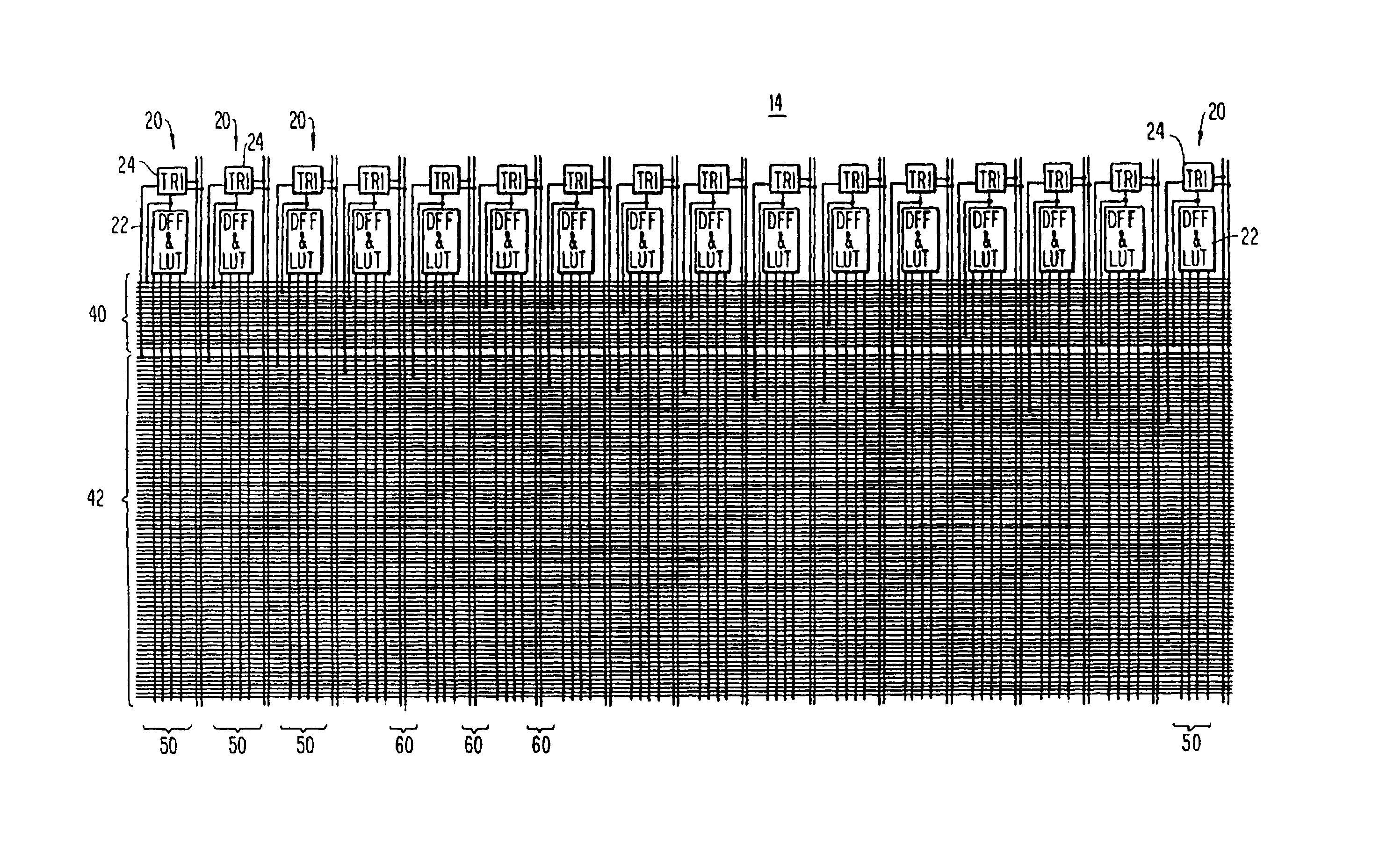
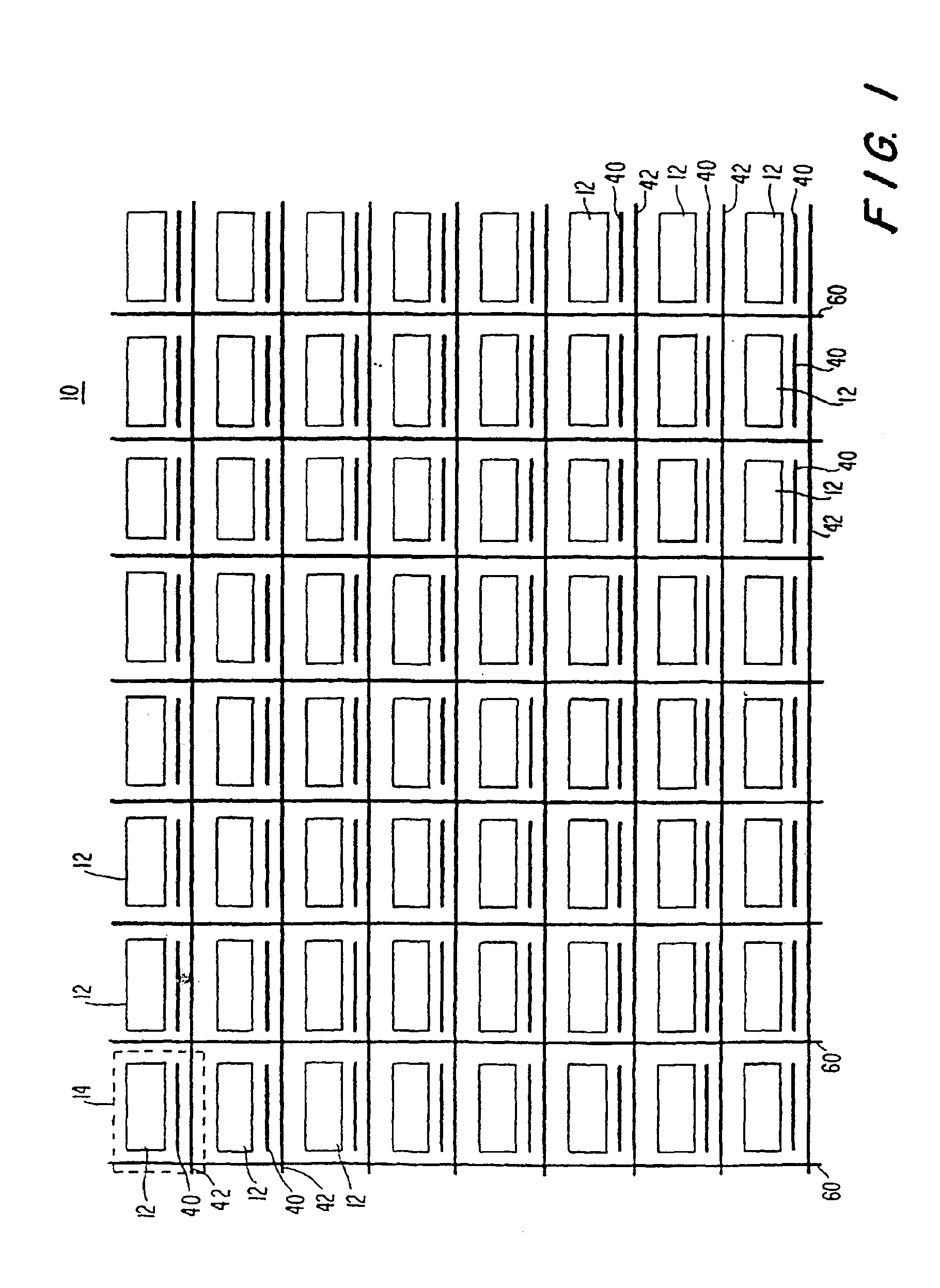
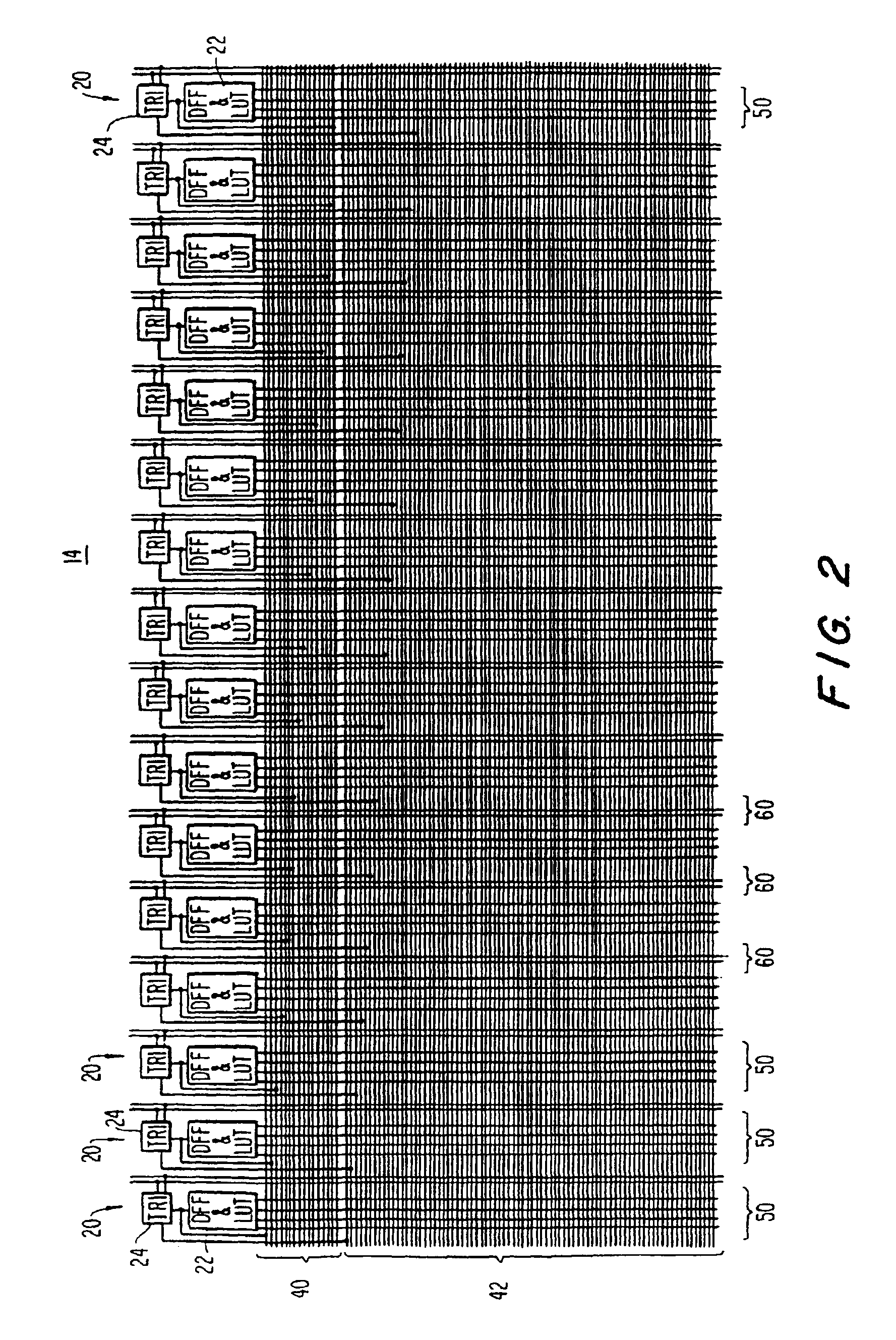
[0048]As shown in FIG. 1, an illustrative programmable logic array integrated circuit 10 constructed in accordance with the first embodiment of the present invention includes a two-dimensional array of groups 12 of programmable logic elements. The representative portion of FIG. 1 which is surrounded by broken line 14 and which includes a typical group 12 is shown in more detail in FIG. 2. The structure shown in FIG. 2 is sometimes referred to herein as a logic array block or LAB. Accordingly, integrated circuit 10 (FIG. 1) is an eight by eight two-dimensional array of sixty-four LABs 14.

[0049]As can be seen in FIG. 2, each LAB 14 includes sixteen programmable logic elements or macrocells 20, a representative one of which is shown in more detail in FIG. 3. In particular, although other types of logic elements could be used instead, in the illustrative embodiment shown in FIG. 3 each programmable logic element 20 includes a D-type flip-flop and four-input look-up ta...

second embodiment

II. Second Embodiment

[0062]FIG. 10 shows the overall organization of an illustrative programmable logic array integrated circuit 210 constructed in accordance with the second embodiment of the present invention. Not all of the conductors employed in circuit 210 are shown in FIG. 10, but enough is shown in this Fig. to begin the discussion. Each logic module 212 is represented by a small square in FIG. 10. Logic modules 212 are grouped together in groups of eight. Each of these groups is referred to as a logic array block or LAB 214. LABs 214 are arranged in six horizontal rows and twenty two vertical columns on circuit 210. Accordingly, there are a total of one hundred thirty-two LABs 214 and one thousand fifty six logic modules 212 on circuit 210. Each logic module 212 is capable of performing a relatively elementary logic function (discussed in more detail below), but extremely complex logic can be performed by variously interconnecting the logic modules as will now be discussed.

[...


PUM


Abstract

A programmable logic array integrated circuit has a number of programmable logic modules which are grouped together in a plurality of logic array blocks (“LABs”). The LABs are arranged on the circuit in a two dimensional array. A conductor network is provided for interconnecting any logic module with any other logic module. In addition, adjacent or nearby logic modules are connectable to one another for such special purposes as providing a carry chain between logic modules and / or for connecting two or more modules together to provide more complex logic functions without having to make use of the general interconnection network. Another network of so-called fast or universal conductors is provided for distributing widely used logic signals such as clock and clear signals throughout the circuit. Multiplexers can be used in various ways to reduce the number of programmable interconnections required between signal conductors.

Description

[0001]This patent application is a continuation of[0002]U.S. patent application Ser. No. 09 / 935,792, filed Aug. 22, 2001, which is a continuation of[0003]U.S. patent application Ser. No. 09 / 496,945, filed Feb. 3, 2000, now abandoned, which is a continuation of[0004]U.S. patent application Ser. No. 09 / 179,254, filed Oct. 26, 1998, now U.S. Pat. No. 6,064,599, which is a continuation of[0005]U.S. patent application Ser. No. 08 / 851,858, filed May 6, 1997, now U.S. Pat. No. 5,848,005 which is a continuation of[0006]U.S. patent application Ser. No. 08 / 655,870, filed May 24, 1996, now U.S. Pat. No. 5,668,771 which is a continuation of[0007]U.S. patent application Ser. No. 08 / 245,509, filed May 18, 1994, now U.S. Pat. No. 5,550,782 which is a continuation-in-part of[0008]U.S. patent application Ser. No. 08 / 111,693, filed Aug. 25, 1993, now U.S. Pat. No. 5,436,575 which is a continuation-in-part of[0009]U.S. patent application Ser. No. 07 / 880,942, filed May 8, 1992, now U.S. Pat. No. 5,260,...

Claims


Application Information

Patent Timeline
Patent Type & Authority Patents(United States)
IPC IPC(8): G11C8/00G11C8/12H03K19/177H03K19/173G01R31/28G01R31/3185
CPCG11C8/12H03K19/17736H03K19/17704H03K19/17728H03K19/1737G01R31/318516
Inventor CLIFF, RICHARD G.COPE, L. TODDMC CLINTOCK, CAMERON R.LEONG, WILLIAMWATSON, JAMES A.HUANG, JOSEPHAHANIN, BAHRAM
Owner ALTERA CORP
Why Eureka
Try Eureka