

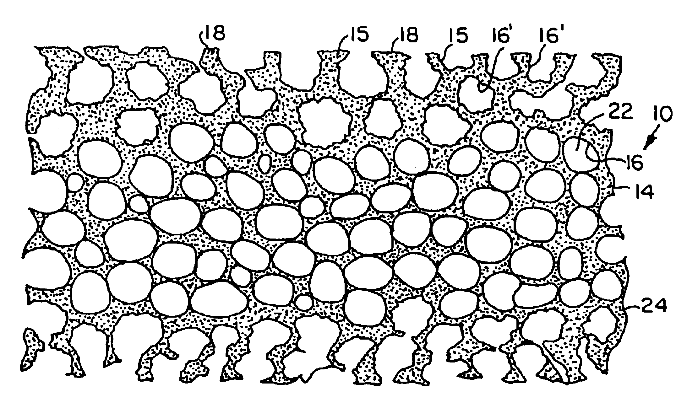
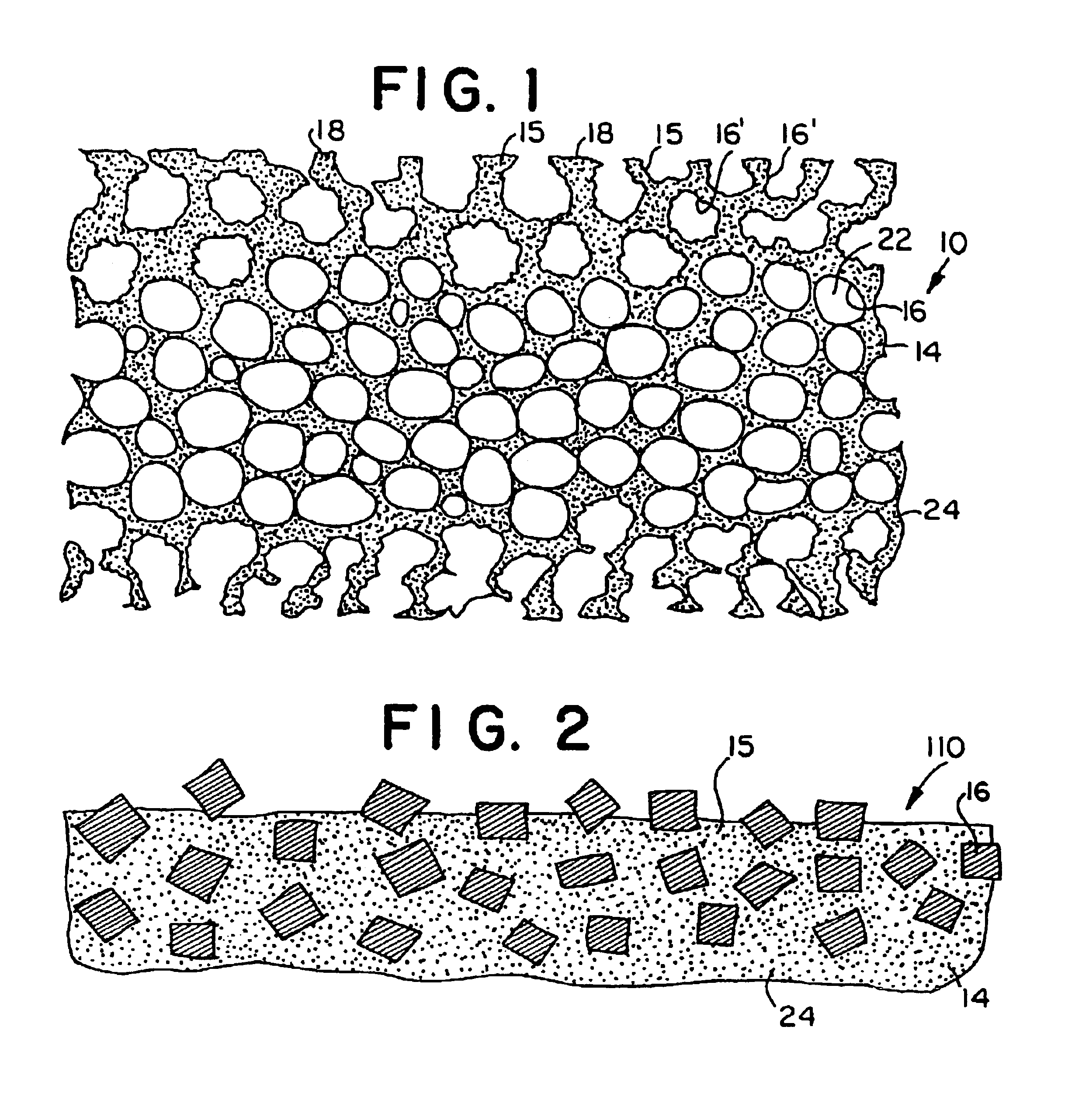
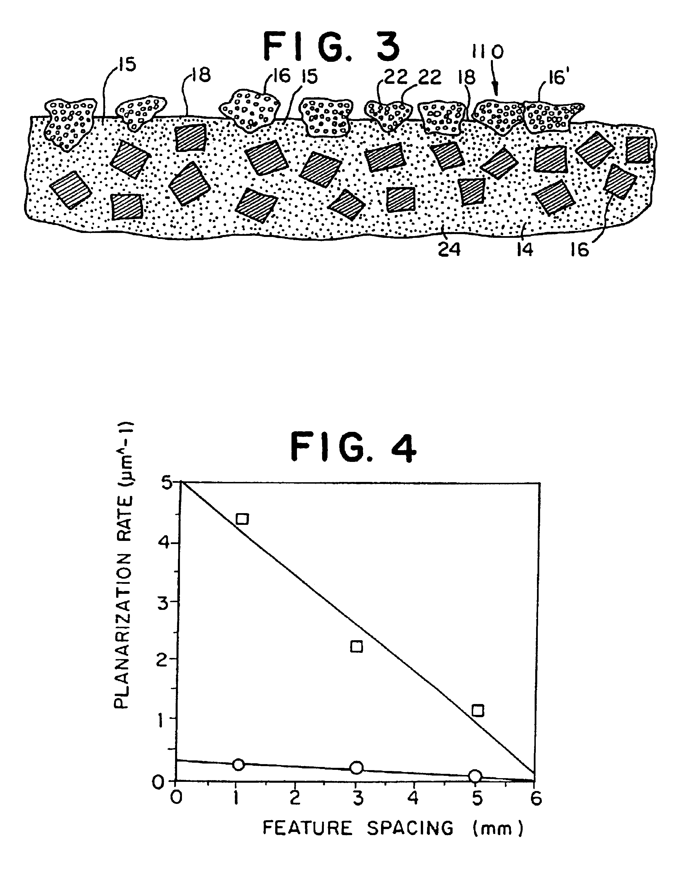
Polishing pad for a semiconductor device having a dissolvable substance
a technology of dissolvable substances and polishing pads, which is applied in the field of polymer substrates, can solve the problems of non-uniform physical properties of polishing pads, stratified substrates, and high wear of the top layer of such stratified pads, and achieve less rigidity, more uniform and consistent polishing of workpieces, and reduce the effect of effective rigidity of the surrounding portion 15
- Summary
- Abstract
- Description
- Claims
- Application Information
AI Technical Summary
Benefits of technology
Problems solved by technology
Method used
Image

Examples
example 1
[0049]A polymeric matrix was prepared by mixing 2997 grams of Uniroyal Adiprene L-325 polyether-based liquid urethane with 768 grams of Curene® 442 (4,4′-methylene-bis [2-chloroaniline] (“MOCA”) at about 150° F. At this temperature, the urethane / polyfunctional amine mixture has a pot life of about 2.5 minutes (the “low viscosity window”).
[0050]During this low viscosity window, 69 grams of EXPANCEL™ 551 DE hollow elastic polymeric microspheres were blended with the polymer mixture at 3450 rpm using Rodel Incorporated high shear blending and mixing equipment to generally evenly distribute the microspheres in the polymer mixture. The mixture was transferred to a conventional mold during the low viscosity window and permitted to gel for about 15 minutes.
[0051]The mold was next placed in a curing oven, such as is commercially available from Koch Oven Corporation. The mixture was cured in the oven for about 5 hours at about 200° F. The power to the oven was then shut off and the mixture p...
example 2
[0054]A polymeric matrix was prepared by mixing 2997 grams of Uniroyal ADIPENE™ L-325 urethane with 768 grams of CURENE® 442 MOCA and high shear mixing the urethane polymer with 87 grams of powdered partially acetylated polyvinyl alcohol, which is commercially available from Air Products and Chemicals Corporation of Allentown, Pa. During the low viscosity window (2.5 mins.), the mixture was poured into a mold, gelled, cured in an oven for about six hours at about 225° F. and cooled to room temperature in a similar manner to that of the article of Example 1. It is believed that essentially no reaction of the OH groups of the polyvinyl alcohol and the isocyanate group of the liquid urethane occurs because of the much faster reaction of the urethane with the MOCA amino groups.
example 3
[0055]A polymeric matrix was prepared in a manner similar to that of Example 1 by mixing 3625 grams of ADIPRENEυ L-213 urethane to 930 grams CURENE® 442 MOCA. During the low viscosity window (about 2.5 mins.), 58 grams of pectin powder, which is commercially available from Freeman Industries, Inc. of Tuckahoe, N.Y., was high shear mixed with the urethane polymer to evenly distribute the pectin powder throughout the urethane mixture. During the low viscosity window (2.5 mins.), the resulting urethane / pectin mixture was poured into a mold, gelled and cured for about six hours at 225° F. and cooled and processed in a manner similar to that set forth in Example 1.
PUM
| Property | Measurement | Unit |
|---|---|---|
| thick | aaaaa | aaaaa |
| thickness | aaaaa | aaaaa |
| size | aaaaa | aaaaa |
Abstract
Description
Claims
Application Information