Substrate and method for producing the same, and thin film structure

a manufacturing method and technology of substrate, applied in the direction of microstructure devices, acceleration measurement using interia forces, instruments, etc., can solve the problems of stress difference, cracks on the oxide film or the other film, stress difference, generated between the oxidized siosub>2/sub>film and another film, etc., to reduce the time required for film formation and reduce the effect of stress differen

Inactive Publication Date: 2005-05-31
MITSUBISHI ELECTRIC CORP
View PDF10 Cites 4 Cited by
  • Summary
  • Abstract
  • Description
  • Claims
  • Application Information

AI Technical Summary

Benefits of technology

[0004]The present invention has been devised to solve the above-mentioned problem, and an object thereof is to provide a substrate capable of reducing a stress difference generating between an oxide film on the substrate and another film formed on the oxide film upon thermal shrinkage and also shortening the time required for film formation at the time of forming a thick oxide film, and a manufacturing method thereof as well as a thin-film structural body.
[0011]According to these aspects, upon thermal shrinkage, stresses, mutually exerted by both of the first and second oxide films, are allowed to have mutually opposite directions so that the both stresses are cancelled by each other, and reduced; thus, it becomes possible to reduce a stress difference generated between the first and second oxide films and another film formed on these oxide films, and consequently to prevent the generation of cracks.
[0012]Moreover, the first oxide film is formed by thermally oxidizing silicon in the substrate main body and the second oxide film is formed by depositing a TEOS oxide film or a high-temperature oxide film thereon; therefore, in a case of forming a thick oxide film used for a base, it becomes possible to shorten the time required for the film formation in comparison with a structure in which the oxide film for a base is formed by using only the first oxide film.

Problems solved by technology

In such a substrate, due to a difference in thermal shrinkage characteristic between the oxide film and another film formed on the oxide film, a stress difference is generated between the oxide film and the other film, for example, after an annealing process, with the result that cracks might generate on the oxide film or the other film, or both of the oxide film and the other film due to the stress difference.
The resulting problem with such a conventional substrate is that a stress difference, generated between the oxidized SiO2 film and another film formed thereon upon thermal shrinkage, tends to become greater.
Moreover, in an attempt to make the film thickness of the oxide film used for the base thicker, there is degradation in the efficiency of the thermally oxidizing process due to the increased film thickness, and it takes a long time to form the oxide film.

Method used


Image

  • Substrate and method for producing the same, and thin film structure
  • Substrate and method for producing the same, and thin film structure
  • Substrate and method for producing the same, and thin film structure

Examples


embodiment 1

[0019]1. Embodiment 1

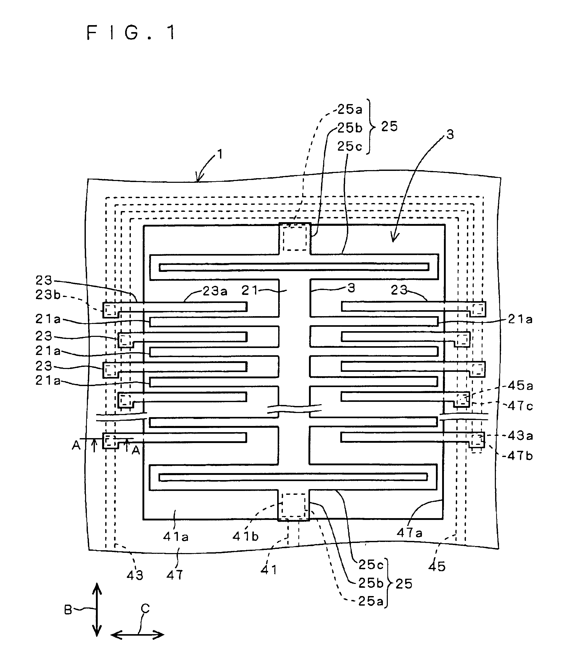
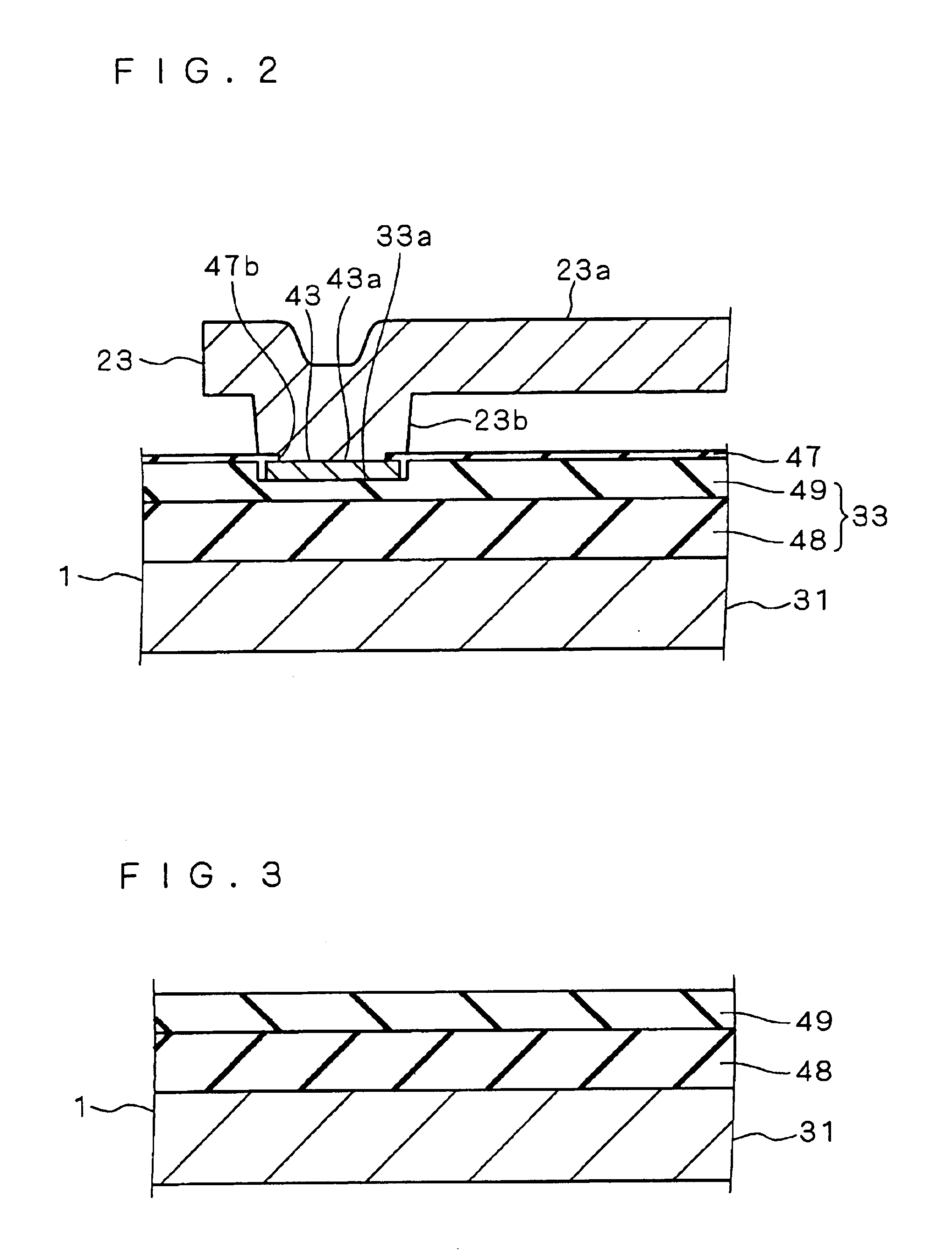
[0020]As shown in FIGS. 1 and 2, a semiconductor acceleration sensor, to which a substrate according to embodiment 1 of the present invention is applied, is provided with a substrate 1 serving as a sensor substrate, and a sensor unit 3 which is formed on the substrate 1 and has a function of detecting acceleration.

[0021]As shown in FIG. 1, the sensor unit 3 is provided with a mass body 21 functioning as a movable electrode, a plurality of fixed electrodes 23 and a plurality of beams 25. The mass body 21, the fixed electrodes 23 and the beams 25, which correspond to the thin-film body of the present invention, are formed by a conductive material, such as doped polysilicon made by doping polysilicon with impurities such as phosphorus.

[0022]The mass body 21 has a plurality of movable electrode portions 21a which are placed with a predetermined gap from the substrate 1, and extend in direction C perpendicular to direction B of acceleration to be detected. The beams ...

embodiment 2

[0039]2. Embodiment 2

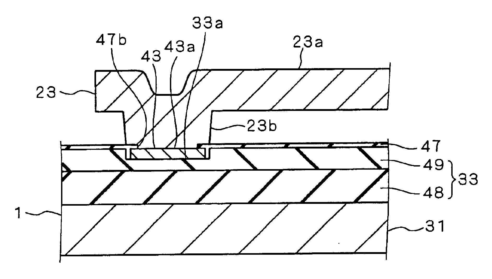
[0040]A substrate 1 according to the present embodiment is substantially different from the substrate 1 of the above-mentioned embodiment 1 only in that the configuration and manufacturing method of the oxide film 33 are different. Therefore, those portions in the substrate 1 of the present embodiment that correspond to those of the substrate 1 according to embodiment 1 are indicated by the same reference numerals, and the description thereof will not be repeated.

[0041]As shown in FIG. 6, in the substrate 1 according to the present embodiment, the oxide film 33 is constituted by a first oxide film 61 made of a thermal SiO2 film that is formed on a substrate main body 31, and a second oxide film 63 made of a high-temperature oxide film deposited and formed on the first oxide film 61. The forming method of the first oxide film 61 is the same as the above-mentioned first oxide film 48. The second oxide film 63 is formed by depositing a high-temperature oxide film t...


PUM

PropertyMeasurementUnit
thicknessaaaaaaaaaa
thicknessaaaaaaaaaa
thicknessaaaaaaaaaa

Abstract

A substrate is provided with a substrate main body made from silicon, and an oxide film for a base formed thereon. The oxide film includes a first oxide film made mainly of a thermal SiO2 film formed by thermally oxidizing silicon in the substrate main body, and a second oxide film made of a high-temperature oxide film deposited and formed thereon. Alternatively the second oxide film may be formed by TEOS.

Description

TECHNICAL FIELD[0001]The present invention relates to a substrate and a manufacturing method thereof as well as a thin-film structural body, and more particularly to a substrate used for an acceleration sensor, and a manufacturing method thereof as well as a thin-film structural body.BACKGROUND ART[0002]The present invention is applied to a substrate which is provided with a substrate main body mainly made of silicon and an oxide film for a base formed on the substrate main body. In such a substrate, due to a difference in thermal shrinkage characteristic between the oxide film and another film formed on the oxide film, a stress difference is generated between the oxide film and the other film, for example, after an annealing process, with the result that cracks might generate on the oxide film or the other film, or both of the oxide film and the other film due to the stress difference.[0003]With respect to this problem, in a conventional substrate, the oxide film used for the base ...

Claims


Application Information

Patent Timeline
Patent Type & Authority Patents(United States)
IPC IPC(8): B81B3/00G01P15/08G01P15/125H01L21/02H01L21/316H01L29/84
CPCB81C1/00365G01P15/0802G01P15/125H01L21/02164H01L21/022H01L21/02238H01L21/02255H01L21/02271H01L21/31612H01L21/31662B81B2201/0235G01P2015/0814B81B2207/07B81C2201/0178B81B2203/0307H01L21/20
Inventor OKUMURA, MIKAHORIKAWA, MAKIOISHIBASHI, KIYOSHI
Owner MITSUBISHI ELECTRIC CORP
Why Eureka
Try Eureka