Method of manufacturing a flash memory cell

Inactive Publication Date: 2005-05-31
SK HYNIX INC
View PDF5 Cites 6 Cited by
  • Summary
  • Abstract
  • Description
  • Claims
  • Application Information

AI Technical Summary

Benefits of technology

[0007]The present invention is contrived to solve the above problems and an object of the present invention is to provide a method of manufacturing a flash memory cell capable of preventing an increase in the thickness of a dielectric film in the annealing process for compensating etch damages after an etch process for forming a stack gate.
[0008]Another object of the present invention is to provide a method of manufacturing a flash memory cell capable of increasing the program / erase speed by increasing the gate-coupling ratio.

Problems solved by technology

Thus, there is a problem that the gate-coupling ratio becomes small and the erase speed is accordingly lowered to degrade the characteristic of the device.

Method used


Image

  • Method of manufacturing a flash memory cell
  • Method of manufacturing a flash memory cell
  • Method of manufacturing a flash memory cell

Examples


Embodiment Construction

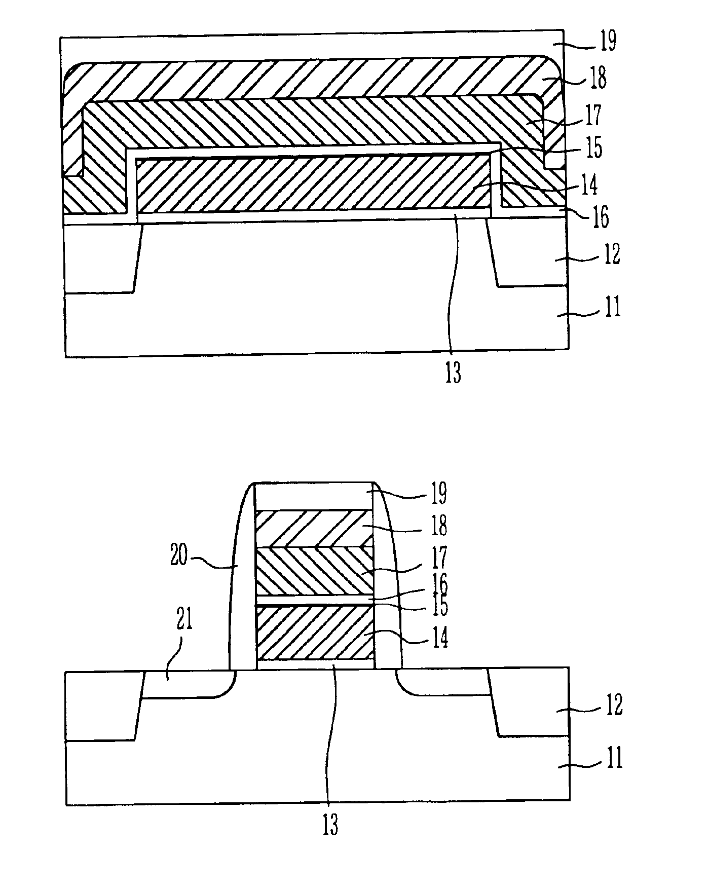
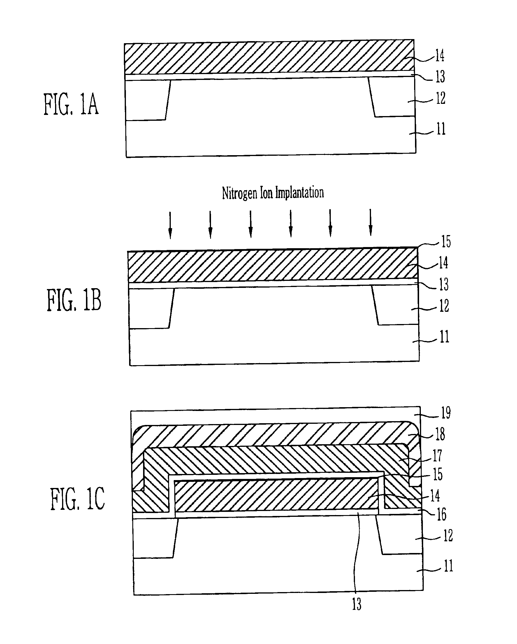
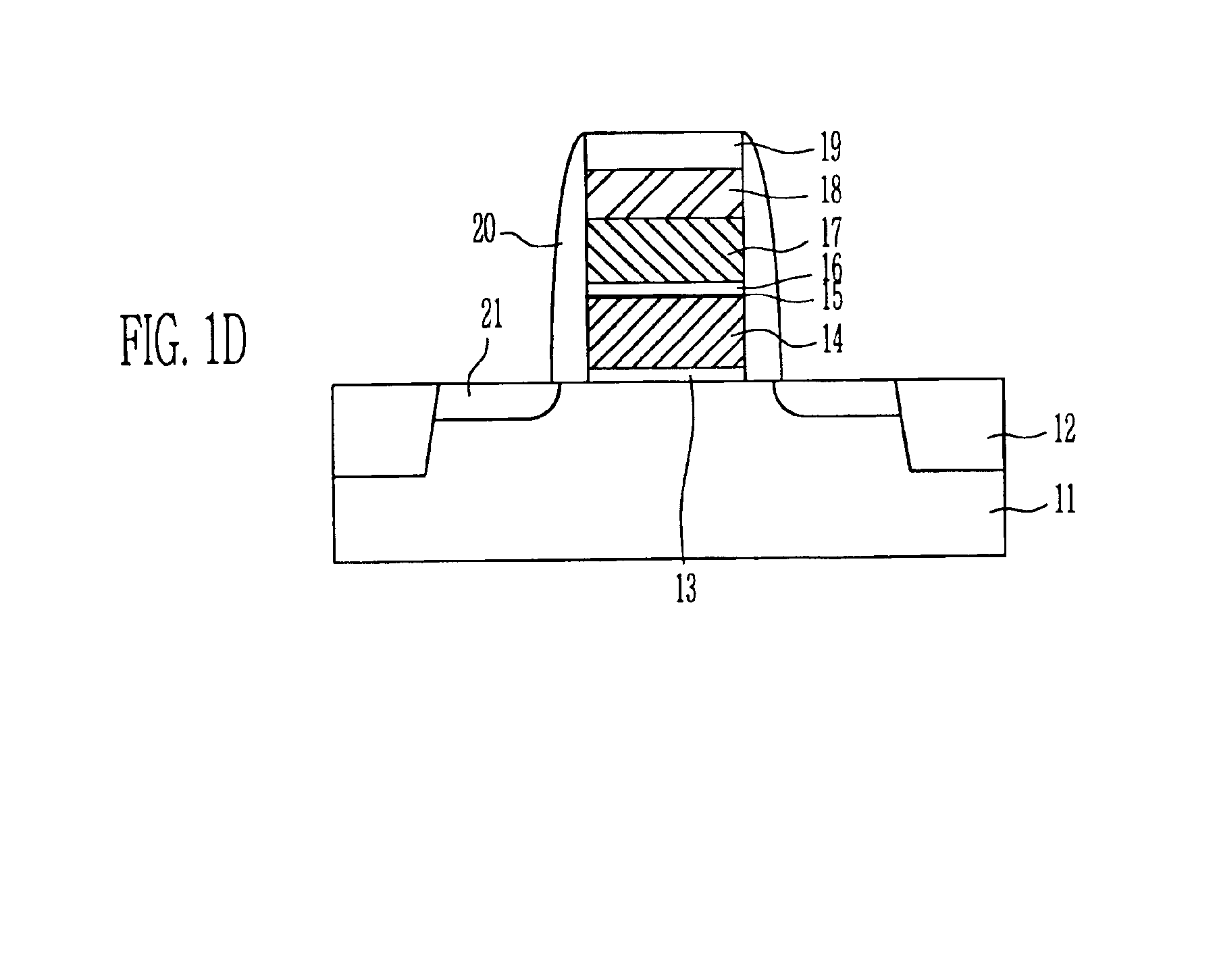
[0012]The present invention will be described in detail by way of a preferred embodiment with reference to accompanying drawings, in which like reference numerals are used to identify the same or similar parts.

[0013]FIG. 1A to FIG. 1D are cross-sectional views of a flash memory cell for explaining a method of the flash memory cell according to the present invention.

[0014]Referring now to FIG. 1A, a trench of a shallow depth is first formed at a given region of the semiconductor substrate 11 and then an insulating film is buried to form a device isolation film 12. Next, a tunnel oxide film 13 and a first polysilicon film 14 are sequentially formed on the entire structure. In the above, the cleaning process is performed before the tunnel oxide film 12 is formed. The cleaning process may be performed using a solution in which a HF diluted to the ratio of 50:1 and a SC-1 (NH4OH / H2O2 / H2O) are compounded or a solution in which a BOE mixed to the ratio of 100:1 or 300:1 and a SC-1 (NH4OH / H...


PUM


Abstract

The present invention relates to a method of manufacturing a flash memory cell capable of preventing an oxidation of a dielectric film between a floating gate and a control gate, in a manner that a polysilicon film for floating gate is deposited, nitrogen ions are injected to make amorphous and contaminate the surface of the polysilicon film.

Description

BACKGROUND OF THE INVENTION[0001]1. Field of the Invention[0002]The invention relates to a method of manufacturing a flash memory cell. More particularly, the present invention relates to a method of manufacturing a flash memory cell capable of preventing an oxidation of a dielectric film between a floating gate and a control gate.[0003]2. Description of the Prior Art[0004]A flash memory cell includes a gate electrode of a stack structure in which a tunnel oxide film, a floating gate, a dielectric film and a control gate are stacked on a given region over a semiconductor substrate, and a junction region on a given region over the semiconductor substrate. A process of manufacturing the flash memory cell will be described below.[0005]The tunnel oxide film and a first polysilicon film are formed on the semiconductor substrate. The first polysilicon film and the tunnel oxide film are then patterned by means of photolithography process and etch process using a given mask. A dielectric fi...

Claims


Application Information

Patent Timeline
IPC IPC(8): H01L21/02H01L21/28H01L21/8247H01L27/115H01L29/788H01L29/792
CPCH01L21/28273H01L29/40114H10B69/00
Inventor DONG, CHA DEOKPARK, SANG WOOK
Owner SK HYNIX INC
Why Eureka
Try Eureka