

Connector receptacle
a technology of connecting receptacles and connectors, which is applied in the direction of coupling device details, coupling device connections, instruments, etc., can solve the problems of difficult design of the pattern layout of the transmission line for data signals, and achieve the effect of reducing the number of parts
- Summary
- Abstract
- Description
- Claims
- Application Information
AI Technical Summary
Benefits of technology
Problems solved by technology
Method used
Image

Examples
embodiment 1
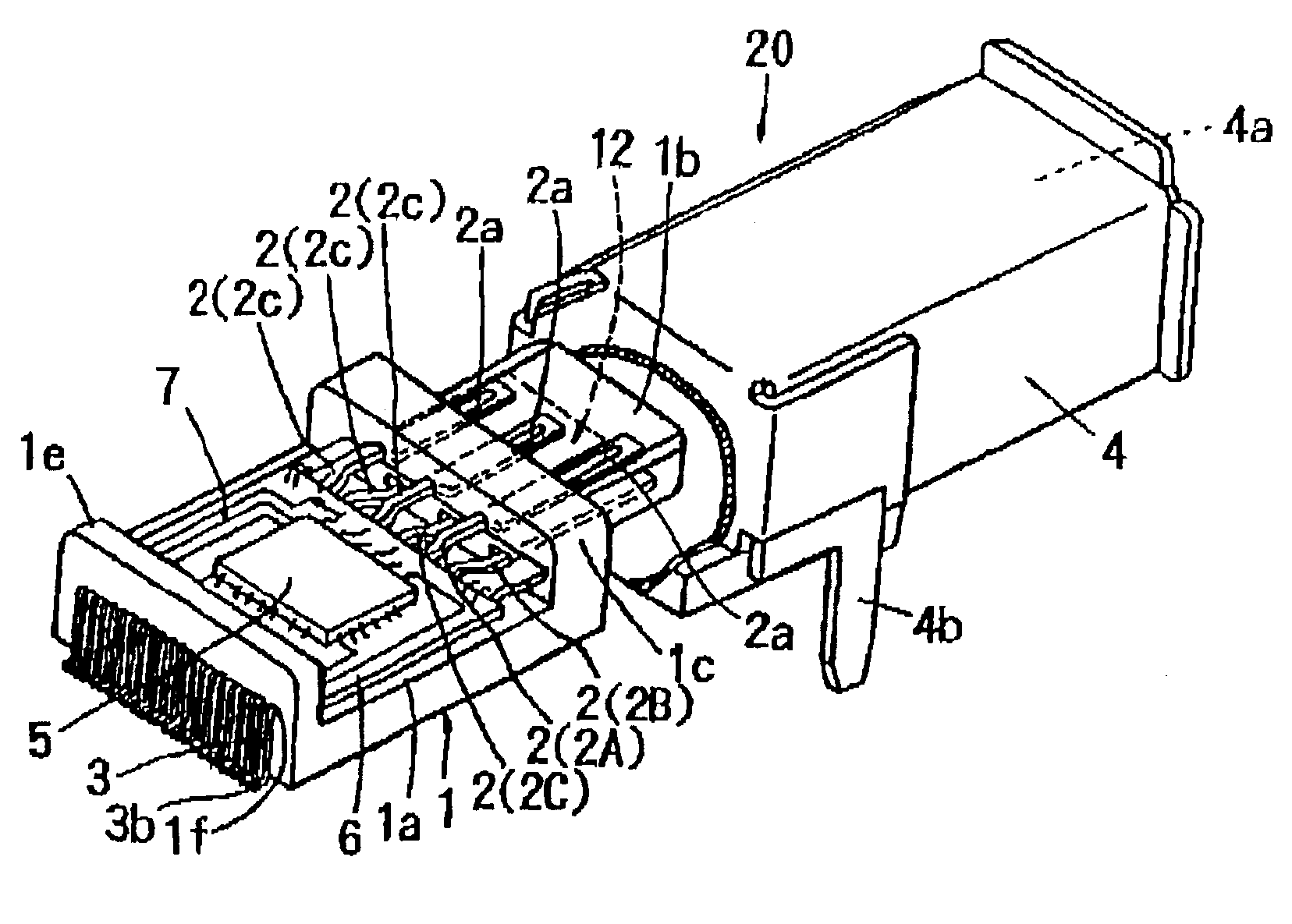
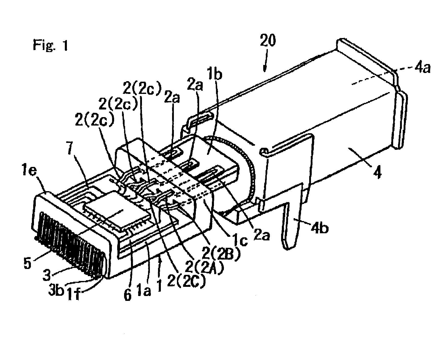
[0037]A connector receptacle according to an embodiment 1 of the present invention will be described in reference to FIGS. 1 to 8. As shown in FIG. 1, the connector receptacle 20 comprises a housing 1, contacts 2, terminals 3, a shell 4, a physical layer basic circuit 5 and a substrate 6. A digital signal is communicated at high speed through the connector receptacle 20.
[0038]The housing 1 is formed of an insulating material and there is provided a substrate bonded portion 1a on which the substrate 6 is bonded by digging its central portion such that its both ends are left. In addition, in the housing 1, a contact supporting portion (Insertion Wafer) 1b to which a connector plug X (not shown) is mated with is extended from its one end.
[0039]The contact 2 is connected from one end portion to a central portion of a connecting portion (not shown) of the connector plug X mate with the contact supporting portion 1b. As shown in FIG. 5, contact touching portions 2a of the contacts 2 which...
embodiment 2
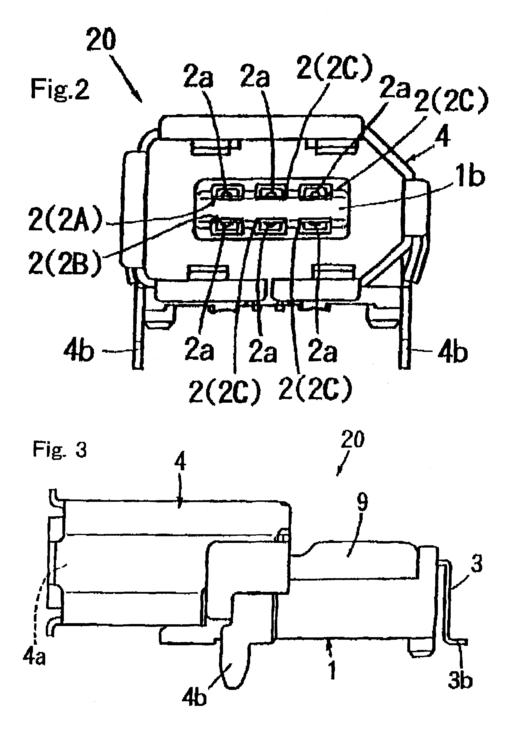
[0055]Then, a connector receptacle according to an embodiment 2 of the present invention will be described in reference to FIGS. 9 to 13. In addition, in FIGS. 9 to 11, a molding resin 9 is not shown. Furthermore, portions substantially having the same functions as in the embodiment 1 are allotted to the same reference numerals and characters and only portions different from those in the embodiment 1 will be described.
[0056]The connector receptacle 20 according to this embodiment of the present invention is basically the same as in the embodiment 1 except that a data signal is communicated in series from contacts 2 to a physical layer basic circuit 5 through transmission lines having almost constant characteristic impedance, and the center of the upper and lower contacts 2 is positioned at almost the same plane as an upper surface of a substrate 6.
[0057]Specifically, as shown in FIG. 12, a contact supporting portion 1b is provided with a ground plane 12 at a central portion in its t...
embodiment 3
[0062]Then, a connector receptacle according to an embodiment 3 of the present invention will be described in reference to FIGS. 14 to 17. In addition, in FIGS. 14 to 16, a molding resin 9 is not shown. Furthermore, portions substantially having the same functions as in the embodiment 2 are allotted to the same reference numerals and characters and only portions different from those in the embodiment 2 will be described.
[0063]The connector receptacle 20 according to this embodiment of the present invention is basically the same as in the embodiment 2 except that a data signal is serially communicated with contacts 2 through patterns 7 serving as transmission lines having almost the same length between the contacts 2 and the physical layer basic circuit 5. In addition, as shown in FIG. 14, there are two contact supporting portions 1b and two shells 4, contacts 2 are provided both upper and lower portions of each of the two contact supporting portions 1b, and the shell 4 extends so as...
PUM
 Abstract
Description
Claims
Application Information