
Vertical type semiconductor device producing apparatus

a semiconductor device and producing apparatus technology, applied in the direction of liquid surface applicators, chemical vapor deposition coatings, coatings, etc., can solve the problems of affecting the processing efficiency of semiconductor devices, etc., to achieve the effect of enhancing the throughpu

Inactive Publication Date: 2005-06-14
KOKUSA ELECTRIC CO LTD
View PDF8 Cites 61 Cited by
  • Summary
  • Abstract
  • Description
  • Claims
  • Application Information

AI Technical Summary

Benefits of technology

[0007]It is a main object of the present invention to provide a vertical type semiconductor device producing apparatus which alternately flows a plurality of kinds of gases which contribute to film formation, and which can enhance the throughput.

Problems solved by technology

According to the conventional ALD apparatus, however, when process gas is supplied to the reaction chamber, since the process gas is supplied while controlling the exhaust amount from the reaction chamber, a gas pressure can not rise in a short time, and there is a defect that the adsorbing speed and reacting speed are slow due to the delay of the gas pressure rise.
In a case of a batch type vertical type ALD apparatus which simultaneously processes a large number of stacked substrates, however, since a capacity of the reaction chamber is large, delay in adsorbing and reacting speed appears remarkably, and there is a problem that throughput is largely deteriorated.
However, the apparatus provided with the gas reservoirs is of single substrate-feeding type in which a capacity of the reaction chamber is small, and the apparatus is not a vertical type apparatus having a large capacity of the reaction chamber.
Further, the apparatus is not the ALD apparatus which alternately supplies process gas a and b into the reaction chamber.

Method used


Image

  • Vertical type semiconductor device producing apparatus
  • Vertical type semiconductor device producing apparatus
  • Vertical type semiconductor device producing apparatus

Examples


Embodiment Construction

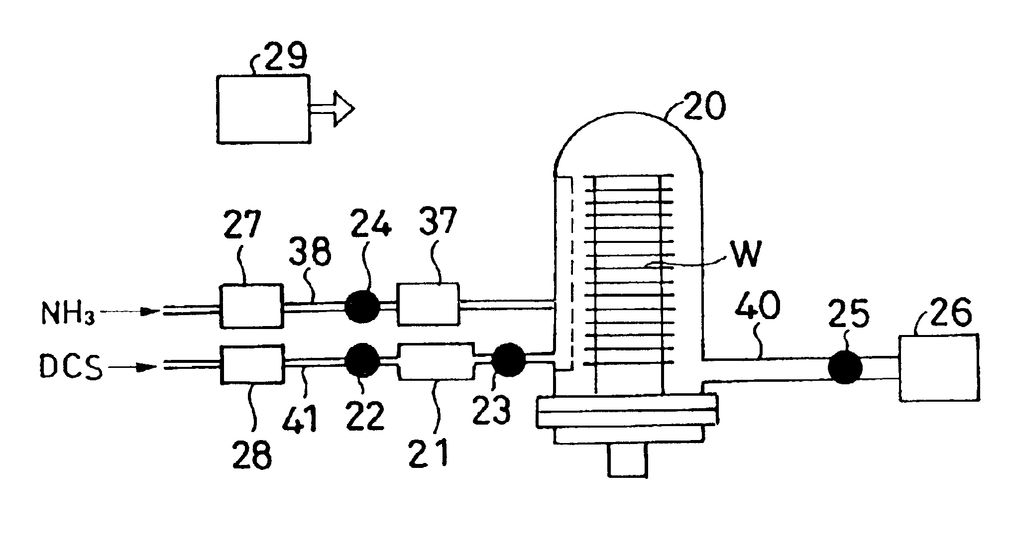
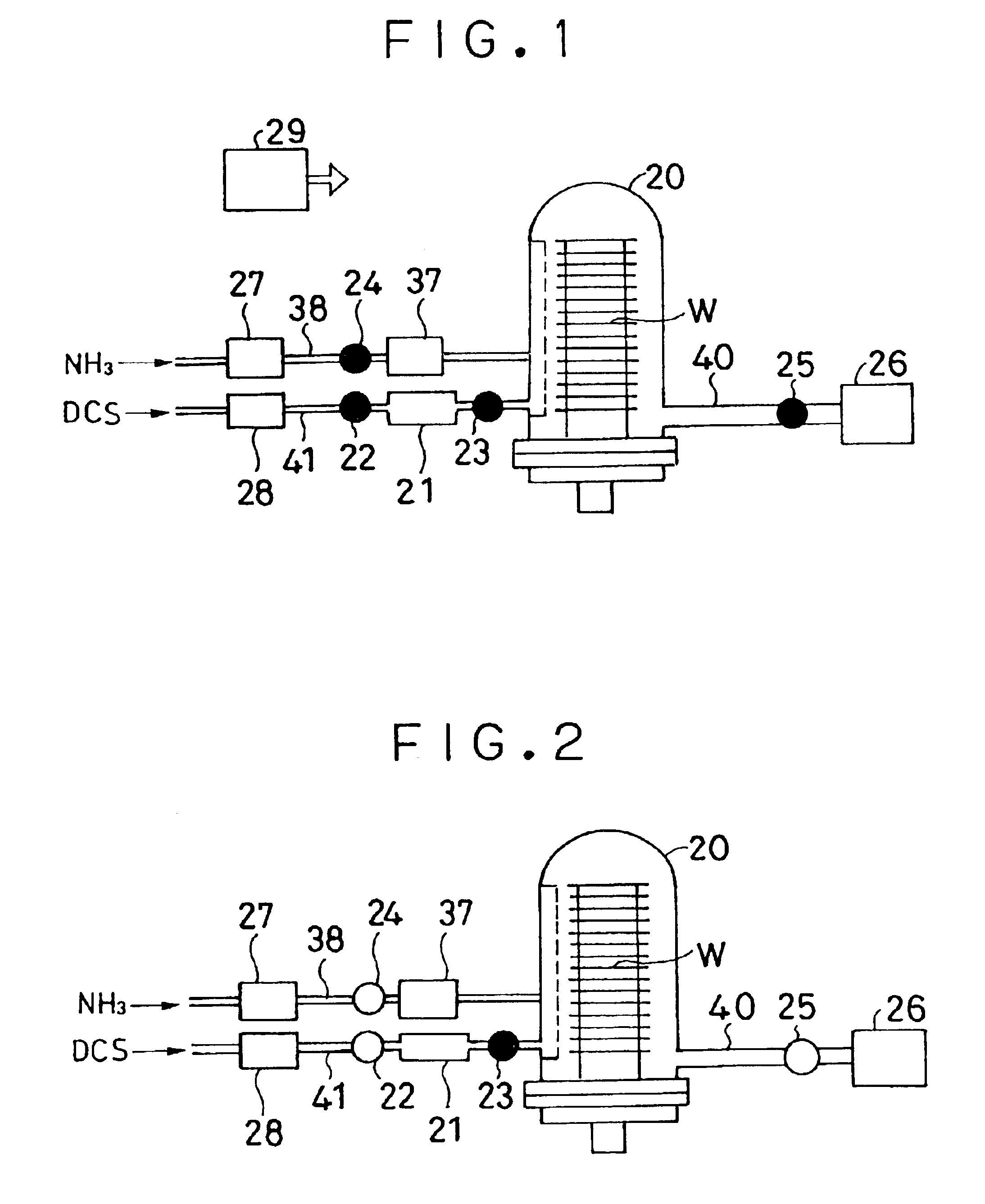
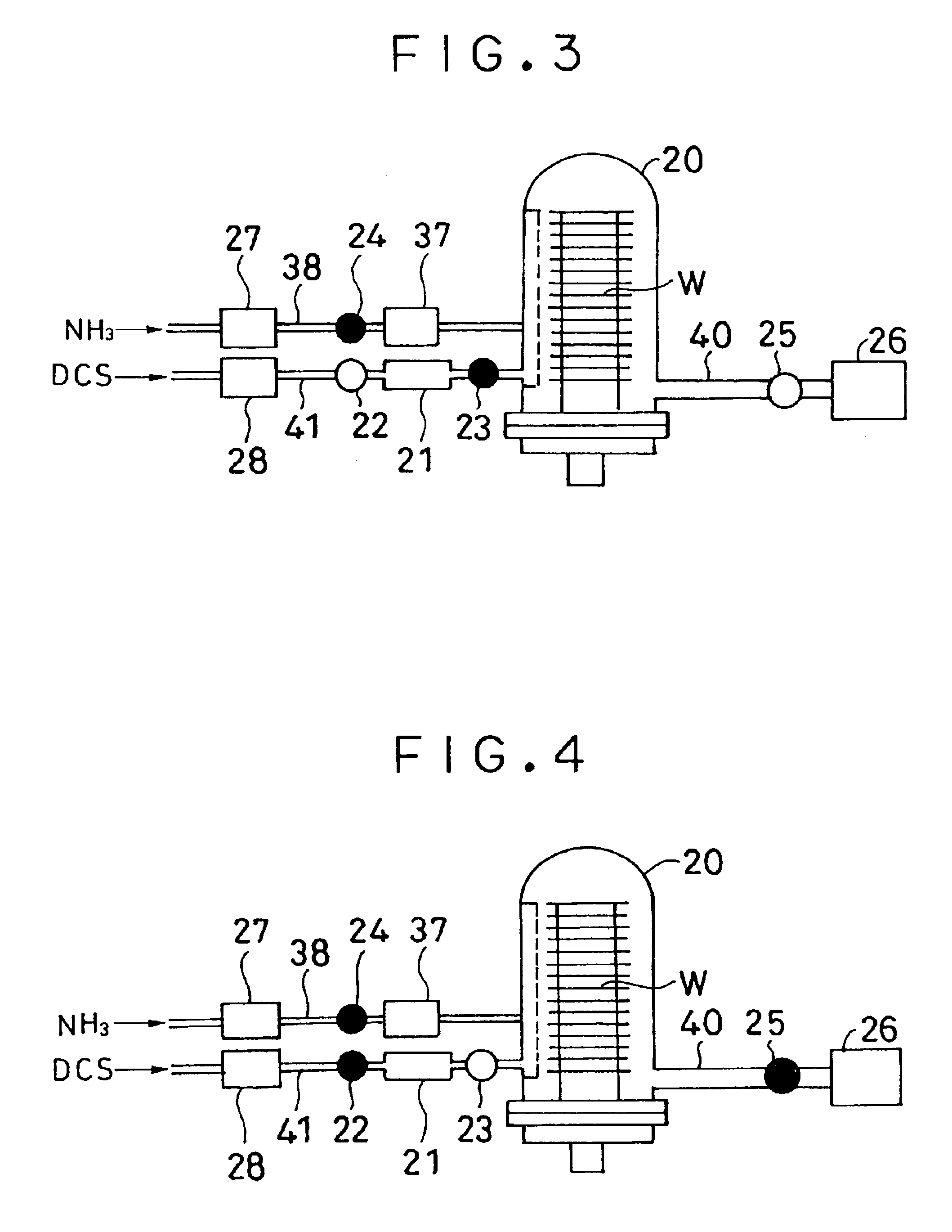
[0025]According to a preferred embodiment of the present invention, there is provided a vertical type semiconductor device producing apparatus, comprising:

[0026]a vertical type reaction chamber which is to accommodate a plurality of stacked substrates;

[0027]an exhaust path which exhausts the reaction chamber,

[0028]a vacuum exhaust device which exhausts the reaction chamber through the exhaust path;

[0029]an exhaust valve which opens and closes the exhaust path;

[0030]a first supply path which supplies a first kind of gas, which contributes to film formation, to the reaction chamber;

[0031]a second supply path which supplies a second kind of gas, which contributes to the film formation, to the reaction chamber;

[0032]a first and a second gas supply valves which respectively open and close the first and second supply paths; and

[0033]a controller which controls the exhaust valve and the first and second gas supply valves such that when the first kind of gas is supplied to the reaction cham...


PUM

PropertyMeasurementUnit
Pressureaaaaaaaaaa
Pressureaaaaaaaaaa
Pressureaaaaaaaaaa

Abstract

A vertical type semiconductor device producing apparatus comprises a vertical type reaction chamber which is to accommodate a plurality of stacked substrates; an exhaust path which exhausts the reaction chamber, a vacuum exhaust device which exhausts the reaction chamber through the exhaust path; an exhaust valve which opens and closes the exhaust path; a first supply path which supplies a first kind of gas, which contributes to film formation, to the reaction chamber; a second supply path which supplies a second kind of gas, which contributes to the film formation, to the reaction chamber; a first and a second gas supply valves which respectively open and close the first and second supply paths; and a controller which controls the exhaust valve and the first and second gas supply valves such that when the first kind of gas is supplied to the reaction chamber, the first kind of gas is supplied to the reaction chamber from the first supply path in a state in which exhaust of the reaction chamber is being stopped to expose the plurality of substrates in the reaction chamber to the first kind of gas, and when the second kind of gas is supplied to the reaction chamber, the second kind of gas is supplied to the reaction chamber through the second supply path in a state in which the reaction chamber is being exhausted by the vacuum exhaust device to expose the plurality of substrates in the reaction chamber to the second kind of gas.

Description

BACKGROUND OF THE INVENTION[0001]1. Field of the Invention[0002]The present invention relates to a vertical type semiconductor device producing apparatus, and more particularly, to a vertical type semiconductor device producing apparatus which alternately flows a plurality of kinds of gases contributing to film formation, and forms films on stacked substrates.[0003]2. Description of the Related Art[0004]FIG. 7 shows an atomic layer deposition apparatus (ALD apparatus, hereinafter) which is a conventional semiconductor device producing apparatus which alternatively flows a plurality of kinds of gases contributing to film formation, and forms films. In this apparatus, two kinds of process gases a and b which contribute to film formation are alternately supplied into a reaction chamber 1, the reaction chamber 1 is exhausted, the gases are adsorbed onto substrates in the reaction chamber 1 and reacted, thereby forming films on the substrates. In this case, a gas supply amount of the pro...

Claims


Application Information

Patent Timeline
IPC IPC(8): C23C16/34C23C16/455C23C16/44
CPCC23C16/345C23C16/45523Y10T29/41C23C16/52C23C16/45536
Inventor OKUDA, KAZUYUKIYAGI, YASUSHIKAGAYA, TORUSAKAI, MASANORI
Owner KOKUSA ELECTRIC CO LTD
Features
  • Generate Ideas
  • Intellectual Property
  • Life Sciences
  • Materials
  • Tech Scout
  • Unparalleled Data Quality
  • Higher Quality Content
  • 60% Fewer Hallucinations
Learn More