Current controlled bridge amplifier

a bridge amplifier and current control technology, applied in the field of electrical circuits, can solve the problems of adversely affecting the high power consumption, and inconvenient operation of the amplifier, and achieve the effect of substantially constant current draw of the amplifier

Inactive Publication Date: 2005-06-14
MICROCHIP TECH INC
View PDF7 Cites 0 Cited by
  • Summary
  • Abstract
  • Description
  • Claims
  • Application Information

AI Technical Summary

Benefits of technology

[0008]In general, the amplifier may be a hybrid amplifier having characteristics of a bridge amplifier and a differential pair amplifier. The amplifier may have a relatively high efficiency while being able to maintain a relatively constant current, thereby reducing or eliminating the generation of unwanted supply current modulation that may cause interference with other nearby circuits.

Problems solved by technology

However, the current draw of this type of amplifier is not constant.
The varying current in such an amplifier may cause interference with other nearby circuits and thus adversely affect their operation.
Furthermore, power transferred to the circuit load is at or near its maximum at nearly all times. Thus, power consumption may tend to be high, and battery life may be adversely impacted.
These inductive loads may require expensive and bulky external components for some lower frequencies.
At higher frequencies, the inductive loads may be integrated onto a die with the rest of the amplifier circuitry, but at the cost of a significant amount of die area.
Alternatively, the inductive loads may be replaced with current sources that may omit the use of inductors, but may reduce the efficiency of the circuit and adversely impact battery life.

Method used


Image

  • Current controlled bridge amplifier
  • Current controlled bridge amplifier
  • Current controlled bridge amplifier

Examples


Embodiment Construction

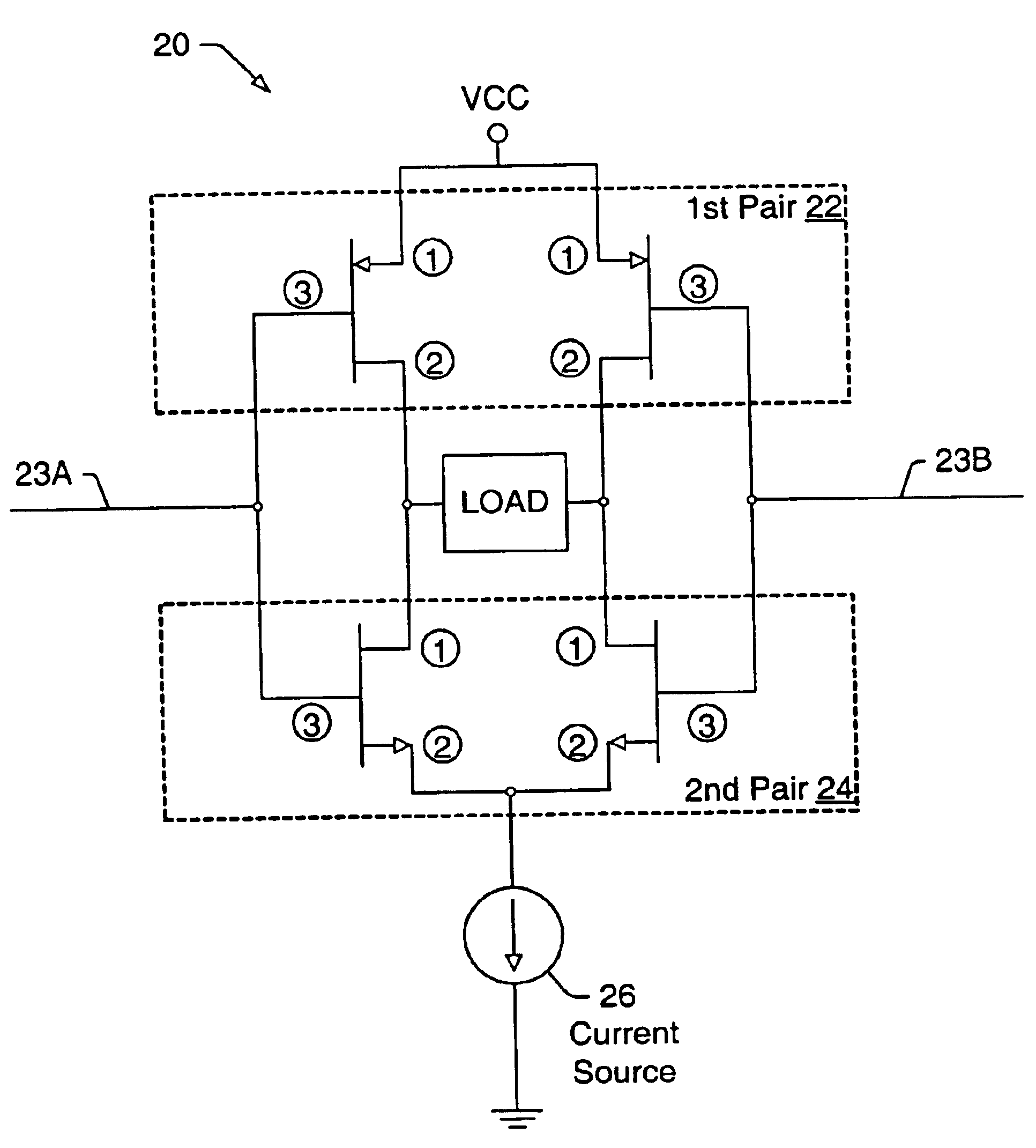
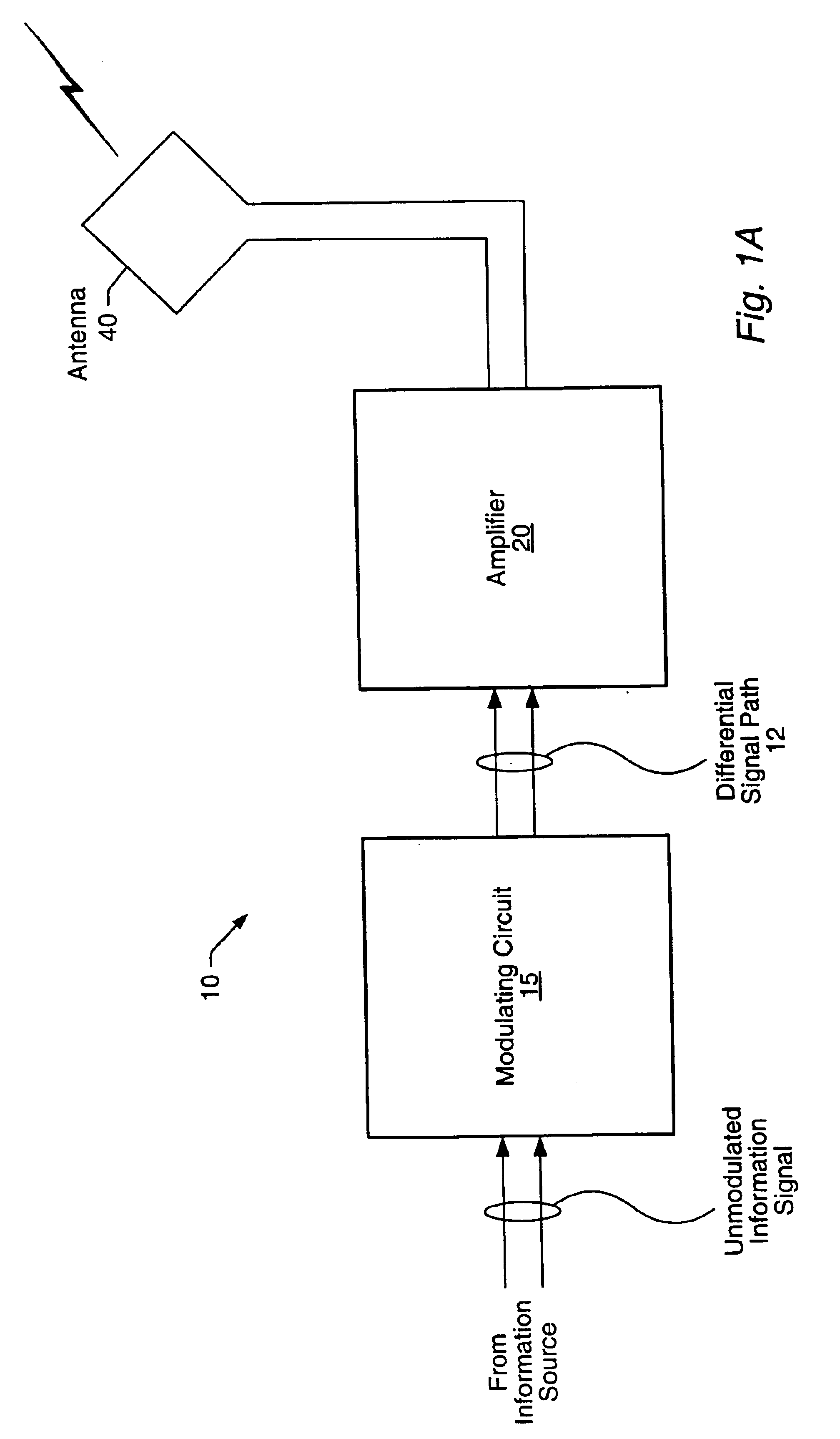
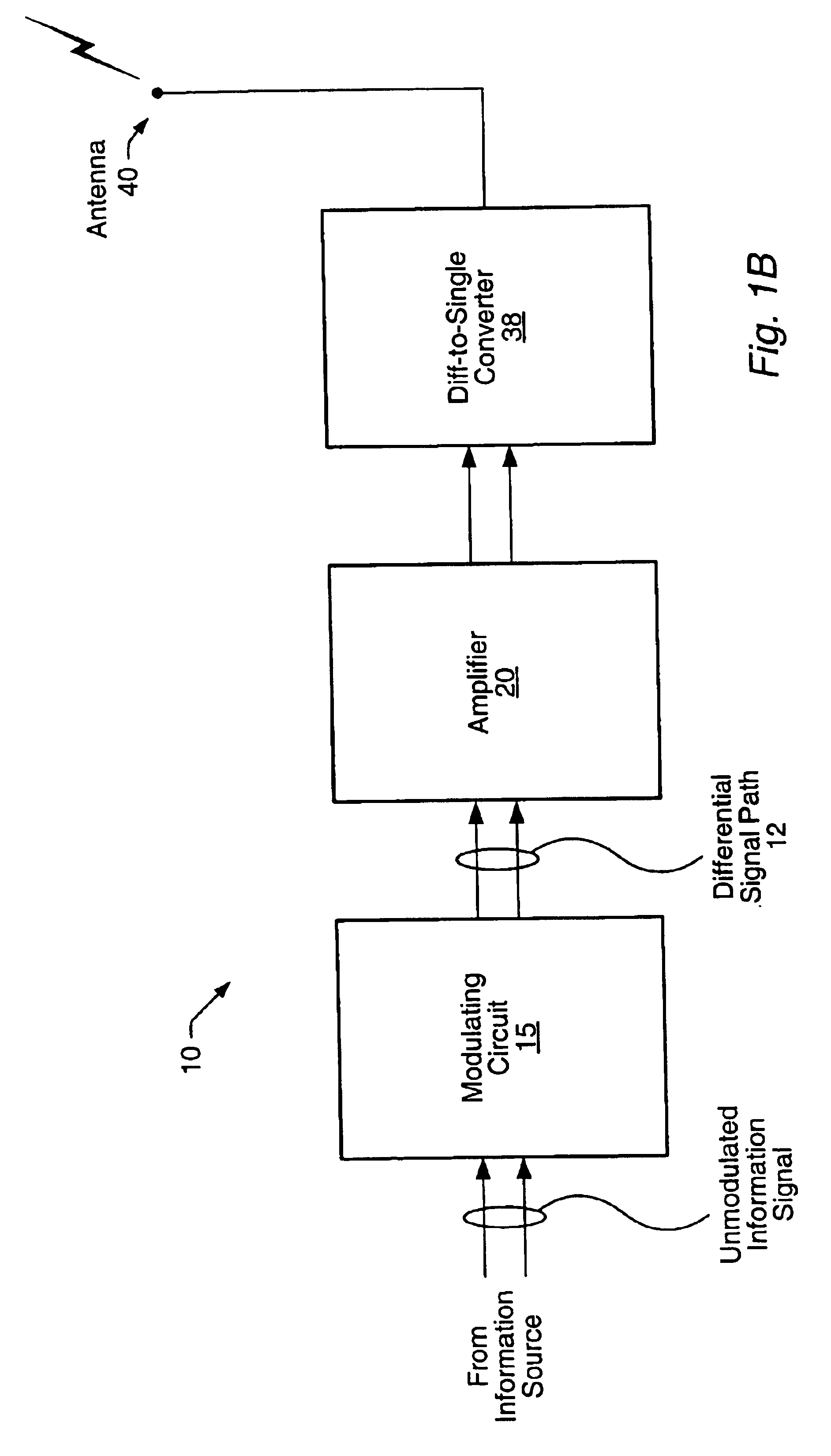
[0016]Turning now to FIG. 1A, a block diagram of one embodiment of a wireless transmission device is shown. Wireless transmission device 10 includes a modulating circuit 15, which is coupled to amplifier 20. It is noted that wireless transmission device 10 may have other components than those explicitly shown here. Amplifier 20 is coupled to antenna 40, which is a loop-type antenna in this particular embodiment. Wireless transmission device 10 may be virtually any type of wireless device configured to transmit signals over the airwaves. For example, wireless transmission device may be a wireless keyboard, a wireless mouse, or a wireless / cordless telephone.

[0017]Modulating circuit 15 may be coupled to receive a differential input signal from an information source. The received information signal may be mixed with a signal at a carrier frequency for transmission from wireless transmission device 10. One of several commonly known modulation techniques may be performed by modulating cir...


PUM


Abstract

An amplifier circuit. In one embodiment, the amplifier includes a first pair of transistors and a second pair of transistors. Each transistor in the amplifier includes a control terminal (e.g. a gate) as well as a first and second terminals. In one embodiment, the transistors are field effect transistors (FETs) and thus the first and second terminals may be either source or drain terminals. First terminals of each of the first pair of transistors may be coupled to a voltage source. The first terminal of each of the second pair of transistors is coupled to the second terminal of one of the first pair of transistors. A current source may be coupled between each of the second terminals and a voltage reference (e.g. ground plane).

Description

FIELD OF THE INVENTION[0001]This invention relates to electronic circuits, and more particularly, to amplifier circuits for transmitting signals in low power wireless devices.DESCRIPTION OF THE RELATED ART[0002]Many portable electronic devices (e.g. cellular telephones, personal digital assistants) operate on battery power. Such battery operated devices need to be prudent with current use. Furthermore, in devices having analog circuitry, interference between circuits must be prevented or minimized.[0003]One of the major consumers of power in portable electronic devices is the transmitter stage amplifier. The transmitter stage amplifier of a wireless device is required to consume enough power for transmitting a signal through the “air” to its intended destination. For non-wireless devices, the transmitter stage may be required to consume enough power to transmit a signal over whatever particular transmission medium is being used.[0004]One type of transmitter amplifier that is commonl...

Claims


Application Information

Patent Timeline
Patent Type & Authority Patents(United States)
IPC IPC(8): H03F3/45
CPCH03F3/45237
Inventor WORTEL, KLAAS
Owner MICROCHIP TECH INC
Why Eureka
Try Eureka