Self-test circuit and memory device incorporating it

Inactive Publication Date: 2005-06-14
SOCIONEXT INC
View PDF3 Cites 100 Cited by
  • Summary
  • Abstract
  • Description
  • Claims
  • Application Information

AI Technical Summary

Benefits of technology

[0026]If a selector circuit is provided in an input circuit as described above, the input circuit inputs an input signal that is changed over by the selector in synchronization with a first clock, while the self-test circuit supplies to the selector a test co

Problems solved by technology

Concomitantly, the cost of the testing step in which inspection for failed bits within the memory is performed using an LSI tester has increased, resulting in increased costs of the memory device.
However, in the above defect testing step, it is necessary to employ an LSI tester, and a long time is required due to the increased capacity of memory.
However, no consensus has yet been reached as to what construction of such a BIST circuit is most suitable.
For example, if a BIST circuit is incorporated in a memory device but simply outputs “pass” or “fail” of the test, it is impossible to ascertain the number of failed bits, and so it is not possible to decide whether or not a rescue function utilizing redundant cells can be utilized.
If, on the other hand, the BIST circuit stores all the addr

Method used


Image

  • Self-test circuit and memory device incorporating it
  • Self-test circuit and memory device incorporating it
  • Self-test circuit and memory device incorporating it

Examples


second embodiment

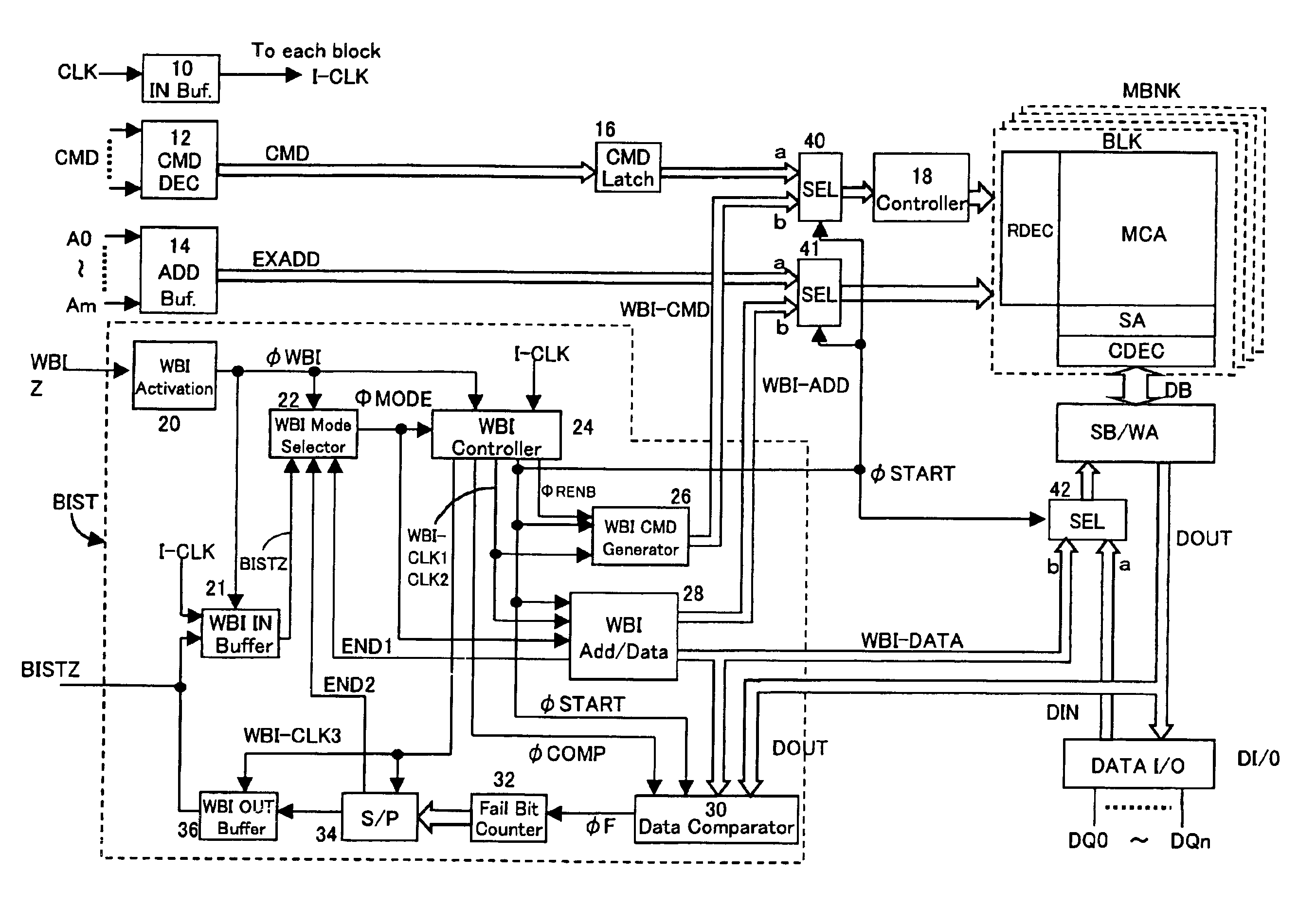
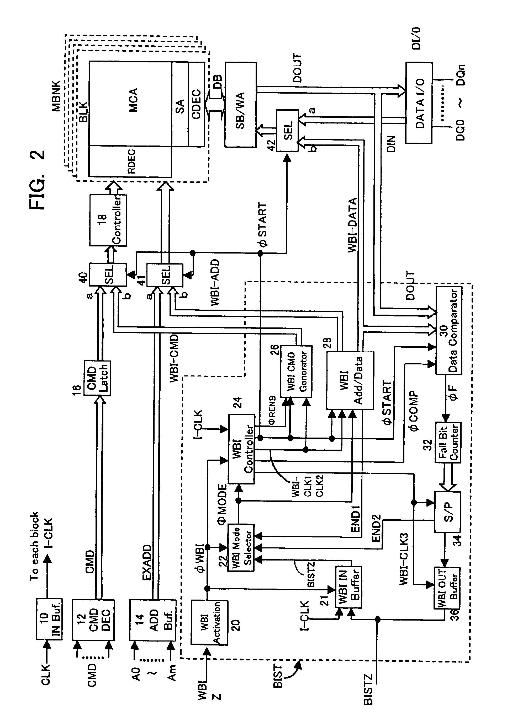
[0114]FIG. 18 is a layout diagram of a memory device according to a second embodiment. In the second embodiment, a clock multiplier circuit 120 is provided on the output side of clock input buffer 10; in the self-test step, a clock CLK2 obtained by multiplying a comparatively slow clock I-CLK2 that is provided from outside is supplied to self-test circuit BIST and the interior of the device. Specifically, a clock CLK of for example 10 MHz is received from outside, and this is multiplied internally to 20 MHz, to operate the internal circuitry at double speed. Also, in this case, interface with the outside is effected by supplying an unmultiplied clock I-CLK 1 to the input / output circuits 21, 36. Also, multiplied clock I-CLK2 could be of three times the speed or four times the speed of external clock CLK.

[0115]The rest of the construction is the same as in the case of the first embodiment shown in FIG. 2. By the provision of a clock multiplier circuit 120 as described above, this self...

third embodiment

[0116]FIG. 19 is a layout diagram of a memory device incorporating a self-test circuit according to a third embodiment. The third embodiment is an example in which the testing can be carried out using the self-test circuit BIST also after assembly into the form of a package. To achieve this, in WBI activation circuit 20, in addition to the activation signal WBIZ in the wafer level burn-in test, a second activation signal WBIZ2 is additionally input from a test mode selection circuit 126 that selects test mode with a special command. When either of these activation signals WBIZ or WBIZ2 is in active condition, WBI activation circuit 20 detects that the self-test step is being performed and makes the internal WBI activation signal øWBI of H level.

[0117]Test mode selector circuit 126 generates the second activation signal WBIZ2 when a specific combination of external command input CMD and / or address input A0 to Am is input. Therefore, self-test circuit BIST is activated in response to ...

fourth embodiment

[0120]FIG. 20 is a layout diagram of a WBI activation circuit and WBI mode selector circuit according to a fourth embodiment. The WBI mode selector circuit in the fourth embodiment is a modification of that of FIG. 3. The WBI mode selector circuit 22 shown in FIG. 20 is provided with flip-flops 134 to 138. These flip-flops input as set / reset signal the pulse generated by pulse generating circuit 130 at the rising edge of WBI activation signal øWBI, and input as data input clock the pulse generated by pulse generating circuit 132 at the rising edge of one or other of the operation mode termination signals END1, 2.

[0121]Consequently, when the WBI activation signal øWBI becomes H level, the flip-flops 134 to 138 sequentially automatically generate test mode signals MODE1→MODE2→MODE3→MODE4→OUTPUT. By utilizing this WBI mode selector circuit, input of the mode signal BISTZ as shown in FIG. 2 or 3 is unnecessary, so the self-test can be executed in an even simpler fashion.


PUM


Abstract

The present invention is a self-test circuit (BIST) incorporated in the memory device, which is activated in response to a test activation signal from outside. When this self-test circuit is activated in response to a test activation signal (WBIZ) from outside, it generates a test operation command (WBI-CMD), generates a test address (WBI-ADD), and generates test data (WBI-DATA). Furthermore, after the self-test circuit writes the test data to a memory cell, it effects a comparison to establish whether or not the read data that is read from this memory cell is the same as the test data that was written thereto and stores information as to the result of this comparison. This comparison result information is then output to the outside.

Description

BACKGROUND OF THE INVENTION[0001]1. Field of the Invention[0002]The present invention relates to a self-test circuit for self-diagnosis incorporated in a memory device and in particular relates to a self-test circuit whereby self-test can be performed utilizing comparatively few input / output terminals. The present invention relates for example to self-test circuits that are suitable for burn-in testing in the wafer processing step.[0003]2. Description of the Related Art[0004]In recent years, memory devices such as dynamic RAM (DRAM) have been increased in capacity and scale. Concomitantly, the cost of the testing step in which inspection for failed bits within the memory is performed using an LSI tester has increased, resulting in increased costs of the memory device.[0005]FIG. 1 is a typical layout diagram of a prior art memory device. FIG. 1 shows a typical layout taking the example of a synchronous DRAM (SDRAM). In the example of FIG. 1, a clock CLK is supplied to clock input buf...

Claims


Application Information

Patent Timeline
IPC IPC(8): G11C29/04G11C29/44G01R31/28G01R31/3185G06F12/16G11C11/401G11C11/407G11C29/00G11C29/06G11C29/12
CPCG11C29/44G11C29/00
Inventor NOMURA, YUKIHIROFUJIMOTO, HIROYUKISUZUKI, TAKAHIROKANDA, TATSUYAMATSUZAKI, YASUROUSAITOU, MASAHIKOTOMITA, HIROYOSHI
Owner SOCIONEXT INC
Why Eureka
Try Eureka