Display unit and drive method therefor

Inactive Publication Date: 2005-06-21
PANASONIC CORP
View PDF14 Cites 41 Cited by
  • Summary
  • Abstract
  • Description
  • Claims
  • Application Information

AI Technical Summary

Benefits of technology

[0024]However, when arranging the circuit of FIG. 34 in the matrix in order to compose an array shown in FIG. 37, it is difficult to adopt the column inversion method or the dot inversion method because of following reason. In case of the column inversion method or the dot inversion method, for instance, in FIG. 37, a scanning electrode G1 is selected, and a pixel (pixel between the scanning electrode G0 and G1) which belongs to this scanning electrode is charged, the pixel is charged with the reversed polarity between adjacent pixels, however, the overlapping voltage supplied from the scanning electrode G0 is the same polarity over all pixels of this line, so the effect of the amplitude increase of the latched voltage of the pixel electrode is not achieved through all pixels.
[0025]FIG. 38 is known as a pixel circuit structure to solve the above-mentioned problem. This is a structure described by page 195 to 198 of Proceedings of the Fourth International Display Workshop. The feature is to invert the layout of the

Problems solved by technology

However, when arranging the circuit of FIG. 34 in the matrix in order to compose an array shown in FIG. 37, it is difficult to adopt the column inversion method or the dot inversion method because of following reason.
An irregular display is a problem along with a demand for increased size and a demand for high resolution of the liquid crystal display.
The first cause of the irregular display is related to the distortion of the scanning voltage waveform caused by the CR time constant of the scanning lines, and the charge of the pixel electrode voltage becoming insufficient by the pixel position.
This is a problem for enlarging and increasing resolution.
Thus, the irregular display is generated by the distortion of the scanning voltage waveform caused by the CR time constant of the scanning line.
The second cause of the irregular display is the re-charge phenomenon caused by the shift of the transistor switching timing because of the distortion of the scanning voltage waveform.
The third cause of the irregular display is a problem that the transistor switch

Method used


Image

  • Display unit and drive method therefor
  • Display unit and drive method therefor
  • Display unit and drive method therefor

Examples


embodiment 1

(Embodiment 1)

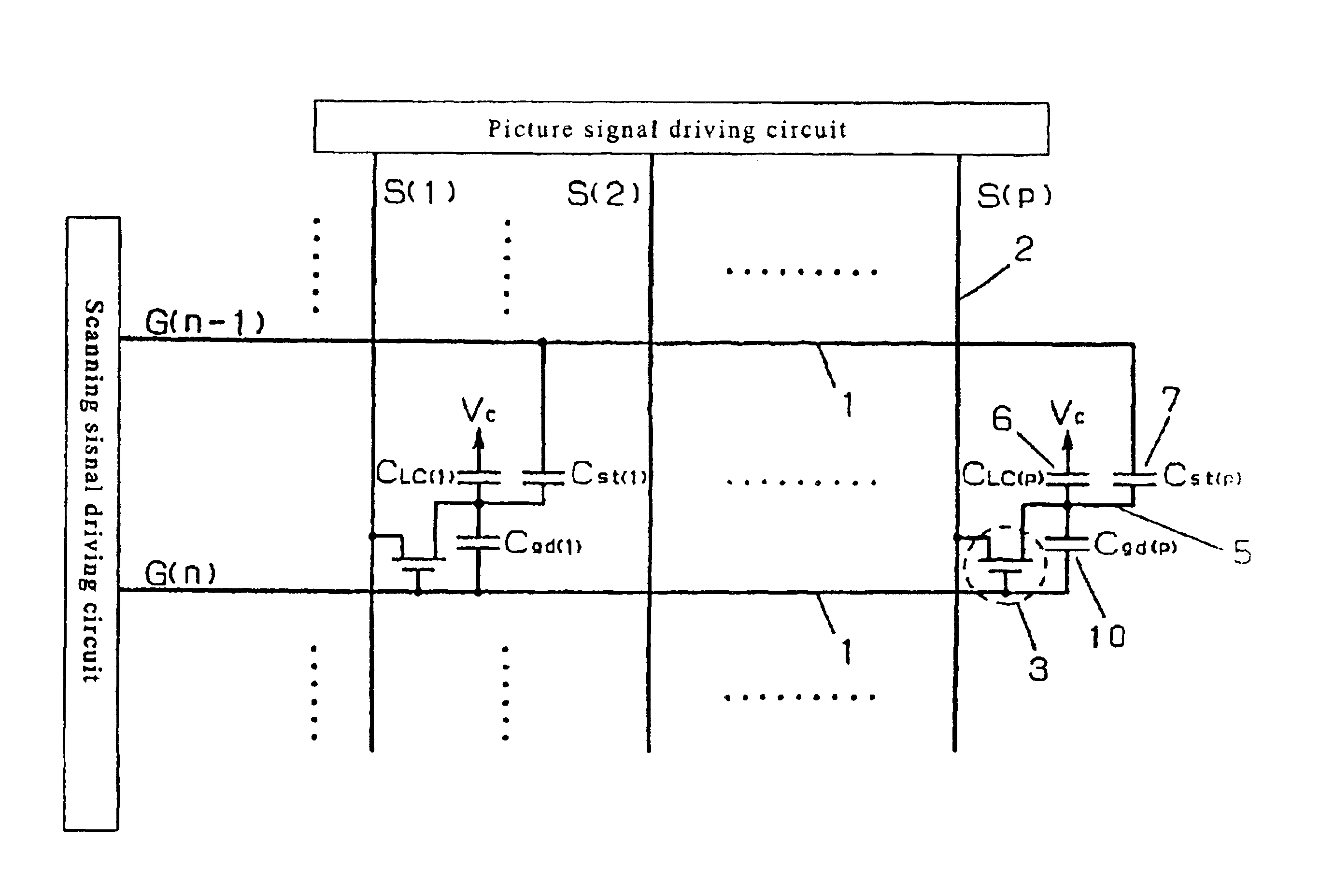
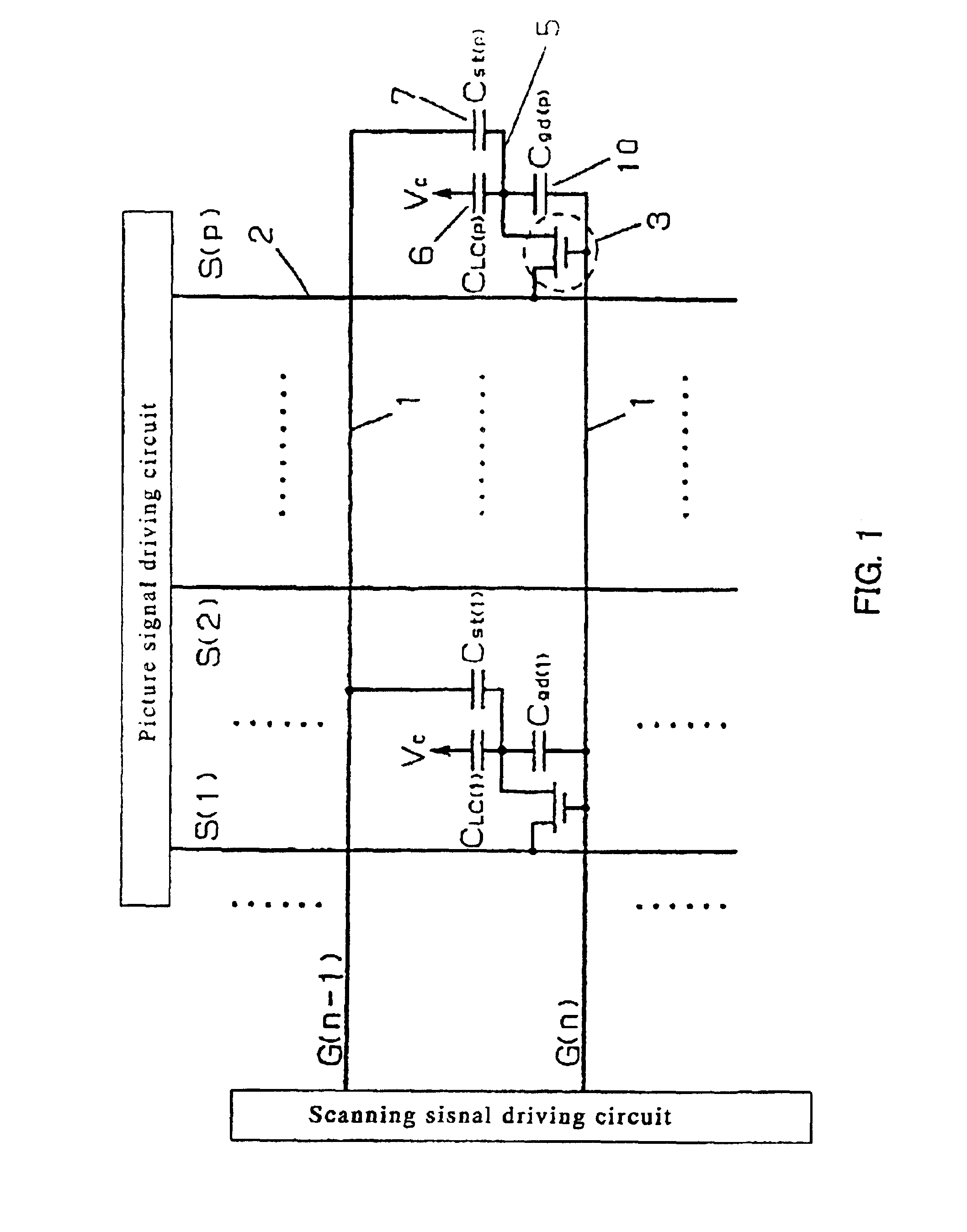
[0179]FIG. 1 is a circuit diagram showing a basic configuration of the liquid crystal display apparatus according to Embodiment 1 of the present invention. In FIG. 1, 1 denotes a scanning electrode, and 2 denotes a picture signal electrode wherein thin film transistor (TFT) 3 is formed at the intersection as a TFT switching element. The gate electrode of TFT 3 is connected with the scanning electrode 1, the source electrode is connected with the picture signal wiring 2, and the drain electrode is connected with the pixel electrode 5 respectively.

[0180]The pixel comprises two capacitor 6 and 7. A liquid crystal capacitor 6 (Clc) is formed between the picture electrode 5 and the opposite electrode, and the liquid crystal is driven by a voltage applied to the both ends. The opposite electrode voltage Vc is supplied to the opposite electrode.

[0181]Storage capacitor 7(Cst) is formed in parallel with the liquid crystal capacitor 6. When the charge leaks from the liquid cryst...

embodiment 3

(Embodiment 3)

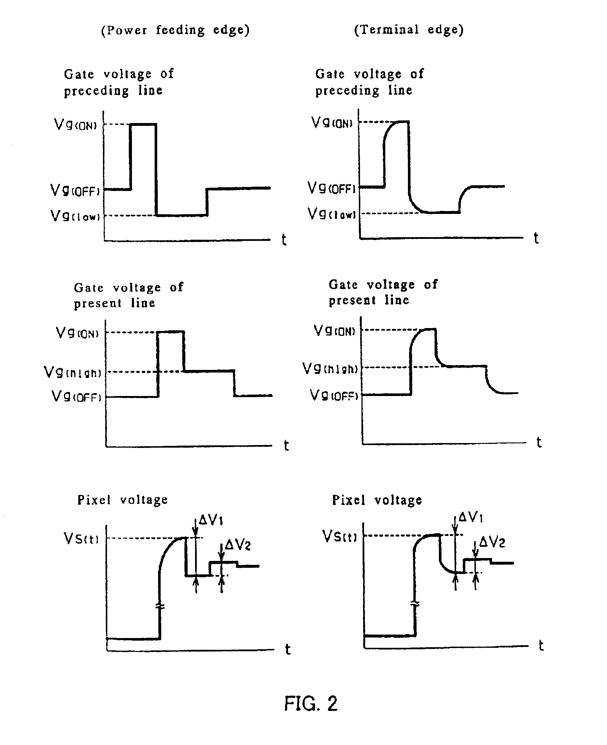
[0219]In Embodiment 1 and Embodiment 2, both the storage capacitance (Cst) and the gate-drain inter-electrode capacitance (Cgd) are gradually enlarged from the power feeding edge of the scanning electrode to the terminal edge. This method gradually enlarges the first capacitance ratio α gd from the power feeding edge of the scanning electrode to the terminal edge by the varying of the gate-drain inter-electrode capacitance, and the varying of the second capacitance ratio α st accompanying the enlargement of α gd is canceled or reduced by the varying of the storage capacitance.

[0220]On the contrary, Embodiment 3 gradually enlarges the first capacitance ratio α gd from the power feeding edge of the scanning electrode to the terminal edge by the varying of the storage capacitance, and the varying of the second capacitance ratio α st accompanying the enlargement of α gd is canceled or reduced by the varying of the gate-drain inter-electrode capacitance.

[0221]The pixel conf...

embodiment 5

(Embodiment 5)

[0237]This Embodiment 5 show an example where the display apparatus shown either in Embodiment 1 to Embodiment 4 is applied to the In-Plane Switching mode (IPS) liquid crystal display apparatus.

[0238]First of all, a basic configuration of the IPS mode liquid crystal display apparatus is described with reference to FIG. 31 and FIG. 32.

[0239]FIG. 31 is a diagram showing a cross section of a IPS liquid crystal display apparatus, and FIG. 32 is a diagram showing a plane configuration of one pixel of the IPS liquid crystal display apparatus. The center part of FIG. 31 shows a cross section structure along A-A′ line shown in FIG. 32.

[0240]In FIG. 31, 11 and 12 are substrates made of glass etc., 11 denotes an array substrate formed with TFTs and electrodes connected with it, and 12 denotes an opposite substrate opposing the array substrate 11. A liquid crystal 13 is inserted between two substrates, and the both ends are sealed by seal 17. 14 and 15 denote polarized light boar...


PUM


Abstract

The present invention provides a display apparatus that can reduce a voltage irregularity and a brightness irregularity accompanied by making an enlarged and a high resolution type display apparatus. The display apparatus comprises plural pixel electrodes 5 arranged in a matrix, a switching element 3 connected with the pixel electrode, a scanning electrode 1, a picture signal electrode 2, an opposite electrode forming a capacitance with the pixel electrode 5, and further comprising; a storage capacitance 7 between the pixel electrode 5 and the scanning electrode 5 other than the scanning electrode 1 of the present line; more than two capacitance elements connected with the pixel electrode 5, including at least one of a gate-drain inter-electrode capacitance 4 of the switching element 3 and the storage capacitance 7, having a different value according to the distance from the power feeding edge of the scanning electrode 1; wherein, each capacitance in each pixel is set so that, when all capacitance connected with the pixel electrode 5 in a pixel is denoted as Ctot, a first capacitance ratio α gd=Cgd/Ctot increases continuously or in stages according to the distance from the power feeding edge of the scanning electrode 1, or a second capacitance ratio α st=Cst/Ctot is substantially constant.

Description

TECHNICAL FIELD[0001]The present invention relates to an active matrix display apparatus using switching devices such as TFT (Thin-Film-Transistor).BACKGROUND ART[0002]The liquid crystal display is widely used for display apparatuses of various electronic equipment as a thin, light type flat display. Especially, the liquid crystal display of the active matrix type, which uses switching element such as TFT, is widely employed into the monitor display for the personal computer and the liquid crystal display television, etc. because of its excellent picture displaying ability.[0003]One of the known methods of driving this active matrix type liquid crystal display is the capacitively coupled driving method disclosed in the unexamined Japanese patent application Tokkai-Hei 2-913 or on page 59-62 of AM-LCD95. This method applies overlapping voltage to the pixel electrode voltage through the capacitive coupling between the storage capacitance and the pixel capacitance. Normally, the storag...

Claims


Application Information

Patent Timeline
IPC IPC(8): G02F1/13G02F1/1362G09G3/36G09G3/32G09F9/33
CPCG02F1/136213G09F9/33G09G3/3208G09G3/3225G09G3/3659G09G3/3648G09G2320/0219G09G2300/0426G09G2300/0842G09G2300/0876G09G2310/0262G09G3/3655G09G3/36
Inventor KUMAGAWA, KATSUHIKOKIMURA, MASANORIFUKAMI, TETSUOTAKIMOTO, AKIOTANAKA, YUKIOKOMORI, KAZUNORI
Owner PANASONIC CORP
Why Eureka
Try Eureka