Signal processing semiconductor integrated circuit device and wireless communication system

Inactive Publication Date: 2005-06-21
RENESAS ELECTRONICS CORP
View PDF11 Cites 59 Cited by
  • Summary
  • Abstract
  • Description
  • Claims
  • Application Information

AI Technical Summary

Benefits of technology

[0021]With the adoption of the control method, in the signal processing semiconductor integrated circuit having the first operation mode in which the reception circuit is activated and the second operation mode in which the reception circuit is deactivated, it will become possible to perform a high-accuracy cal

Problems solved by technology

However, it was found that the direct conversion system has a deficiency that if there is a DC offset in the reception circuit, the DC offset is amplified and outputted.
Therefore, if there are DC offsets on the outputs of each stages,

Method used


Image

  • Signal processing semiconductor integrated circuit device and wireless communication system
  • Signal processing semiconductor integrated circuit device and wireless communication system
  • Signal processing semiconductor integrated circuit device and wireless communication system

Examples


Embodiment Construction

[0034]The preferred embodiments of the invention will now be described with reference to the accompanying drawings.

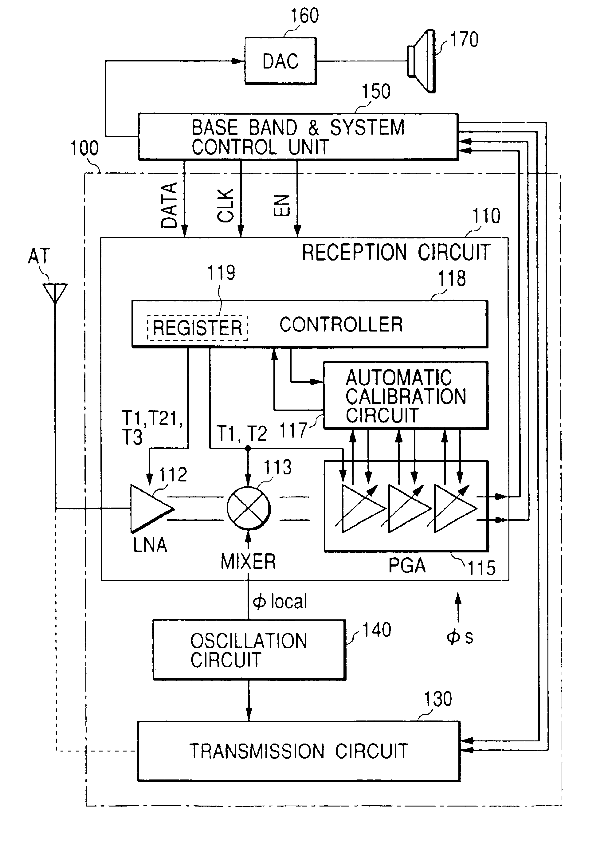
[0035]FIG. 1 illustrates a configuration of a signal processing system for a portable telephone, which is a preferred embodiment for the application of the invention.

[0036]In FIG. 1, AT signifies a transmission / reception antenna for communication radio waves, 110 a reception circuit of the direct conversion system that demodulates a signal received by the antenna AT without intervention of the intermediate frequency, and amplifies and converts the demodulated into a base band signal, 130 a transmission circuit that modulates the base band signal to be transmitted from the antenna AT and converts the frequency, 140 an oscillation circuit that generates the local oscillation signal φ local that is essential to the frequency conversion in the reception circuit 110 and the transmission circuit 130, 150 a base band & system control unit that implements a signal processing su...


PUM


Abstract

The invention provides a signal processing semiconductor integrated circuit of the direct conversion system, which includes a dummy amplifier having the same circuit configuration as a low noise amplifier being the first stage amplifier, in which the DC offset calibrations on the subsequent stage amplifiers are carried out during shifting into the reception mode in a state that the low noise amplifier is deactivated and the dummy amplifier is activated. Thereby, the invention achieves to suppress generation of the DC offsets resulting from the leakage noises of the local oscillator during shifting into the reception mode, and to enhance the reception sensitivity.

Description

BACKGROUND OF THE INVENTION[0001]The present invention relates to a technique effective for use in reducing a DC offset of a multi-stage connection amplifier in a semiconductor integrated circuit, specifically to a signal processing LSI (Large Scale Integrated semiconductor circuit) of the direct conversion system that processes transmission / reception signals, which is used in a portable telephone, for example.[0002]Traditionally, the so-called super-heterodyne system is adopted by a wireless communication LSI that processes transmission / reception signals, which is used in a portable telephone. As a reception circuit of the super-heterodyne system, the construction as shown in FIG. 10 can be put forth as an example. That is, the reception circuit includes a band restriction filter (FLT) 111 made up with a SAW filter that rejects spurious waves from signals received by an antenna AT, a low noise amplifier (LNA) 112 that amplifies a signal passed through the filter 111, a mixer (MIX) ...

Claims


Application Information

Patent Timeline
IPC IPC(8): H03D7/14H04B1/30H04B1/3822H04B1/40
CPCH03D7/1433H04B1/30H03D7/1458H03D2200/0033H03D2200/0047H03D2200/009
Inventor HAYASHI, NORIOHAGINO, NORIYOSHIMATSUI, TOSHIKIWATANABE, KAZUOTANAKA, SATOSHI
Owner RENESAS ELECTRONICS CORP
Why Eureka
Try Eureka