
Integrated process for fuse opening and passivation process for CU/LOW-K IMD

a technology of integrated circuit and passivation process, which is applied in the direction of semiconductor devices, semiconductor/solid-state device details, electrical equipment, etc., can solve the problems of increasing strict limitations on the technology used for semiconductor device creation, device feature size, and conventional approach to creating poly fuse, so as to improve overall semiconductor package reliability, reduce the number of photoresist and etching steps, and no additional manufacturing cost

Inactive Publication Date: 2005-06-28
TAIWAN SEMICON MFG CO LTD
View PDF5 Cites 29 Cited by
  • Summary
  • Abstract
  • Description
  • Claims
  • Application Information

AI Technical Summary

Benefits of technology

[0015]A principle objective of the invention is to provide a process flow for the creation of fuse access and access to a bond pad in which the number of photoresist and etching steps is reduced.
[0016]Another objective of the invention is to provide a process for the creation of a bond pad opening, whereby bonding between the non-exposed surface of the bond pad and surrounding layers of insulating material is improved.
[0017]Yet another objective of the invention is to improve overall semiconductor package reliability in creating fuse access and a bond pad at no additional manufacturing cost incurred by avoiding an increase in the required number of device exposures and the therewith associated use of exposure masks.
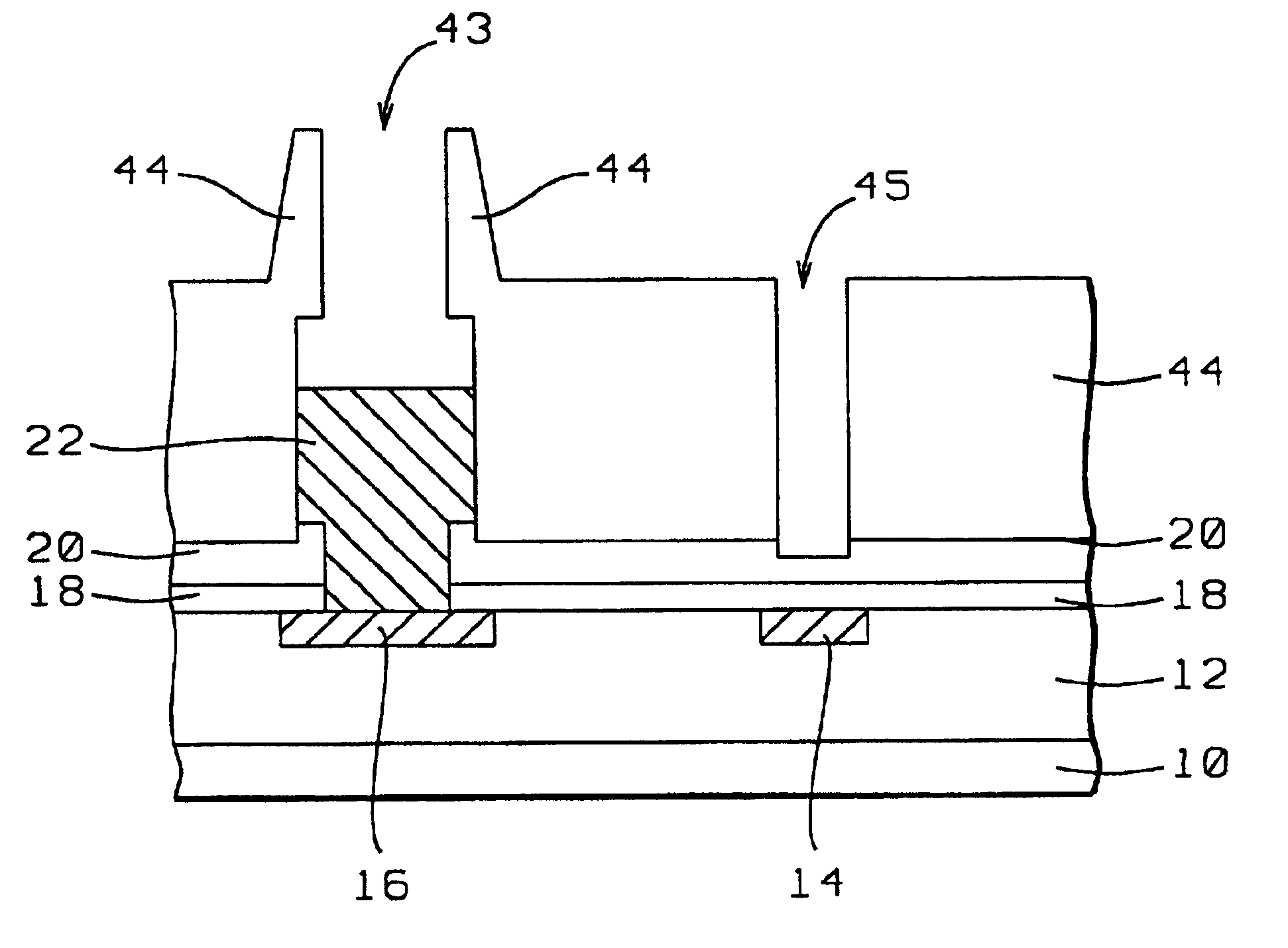
[0018]In accordance with the objectives of the invention a new process flow is provided for the creation of a fuse contact and a bond pad. The invention starts with a semiconductor substrate over the surface of which semiconductor devices, components and conductive interconnects have been created, including top level metal and fuse metal in the surface of a layer of insulation deposited over the surface of the substrate. A first etch stop layer is deposited over the surface of the layer of insulation over which a first passivation layer is deposited, an opening is created through these layers exposing the top level metal. A metal plug is created overlying the exposed surface of the top level metal. A stack of a patterned and etched hard mask layers, having been deposited at part of the creation of the metal plug and overlying a layer of metal plug material, remains in place over the surface of the created metal plug. A second layer of passivation material is deposited over the surface of the structure, the second layer of passivation is patterned and etched exposing the surface of the first layer of passivation overlying the fuse metal and exposing the surface of the stack of hard mask layers overlying the created metal plug. The stack of hard mask layers is then removed from the surface of the metal plug, exposing the surface of the metal plug to serve as a contact pad and further reducing the thickness of the first layer of passivation over the surface of the fuse metal, making the fuse more accessible for fuse blowing.

Problems solved by technology

The therefrom following sharp reductions in device feature size imposes increasingly strict limitations on the technologies that are used for semiconductor device creation.
With the increased number of overlying layers of insulation and with the reduction in device feature size, the conventional approach of creating a poly fuse, that is accessed via an opening created through the layers of insulation, becomes less attractive and has therefore been replaced with the creation of metal fuses.
The laser technology that is used for opening (or blowing) the fuse combined with the characteristics of the typically used low-K dielectrics that are used for the layers of insulation, readily and frequently lead to the occurrence of cracks in the remaining overlying layer of insulation, leading to increased product loss.
An additional concern is the complexity of the process that is required in order to create the layers of interconnect traces in combination with electrical fuse capability.

Method used


Image

  • Integrated process for fuse opening and passivation process for CU/LOW-K IMD
  • Integrated process for fuse opening and passivation process for CU/LOW-K IMD
  • Integrated process for fuse opening and passivation process for CU/LOW-K IMD

Examples


Embodiment Construction

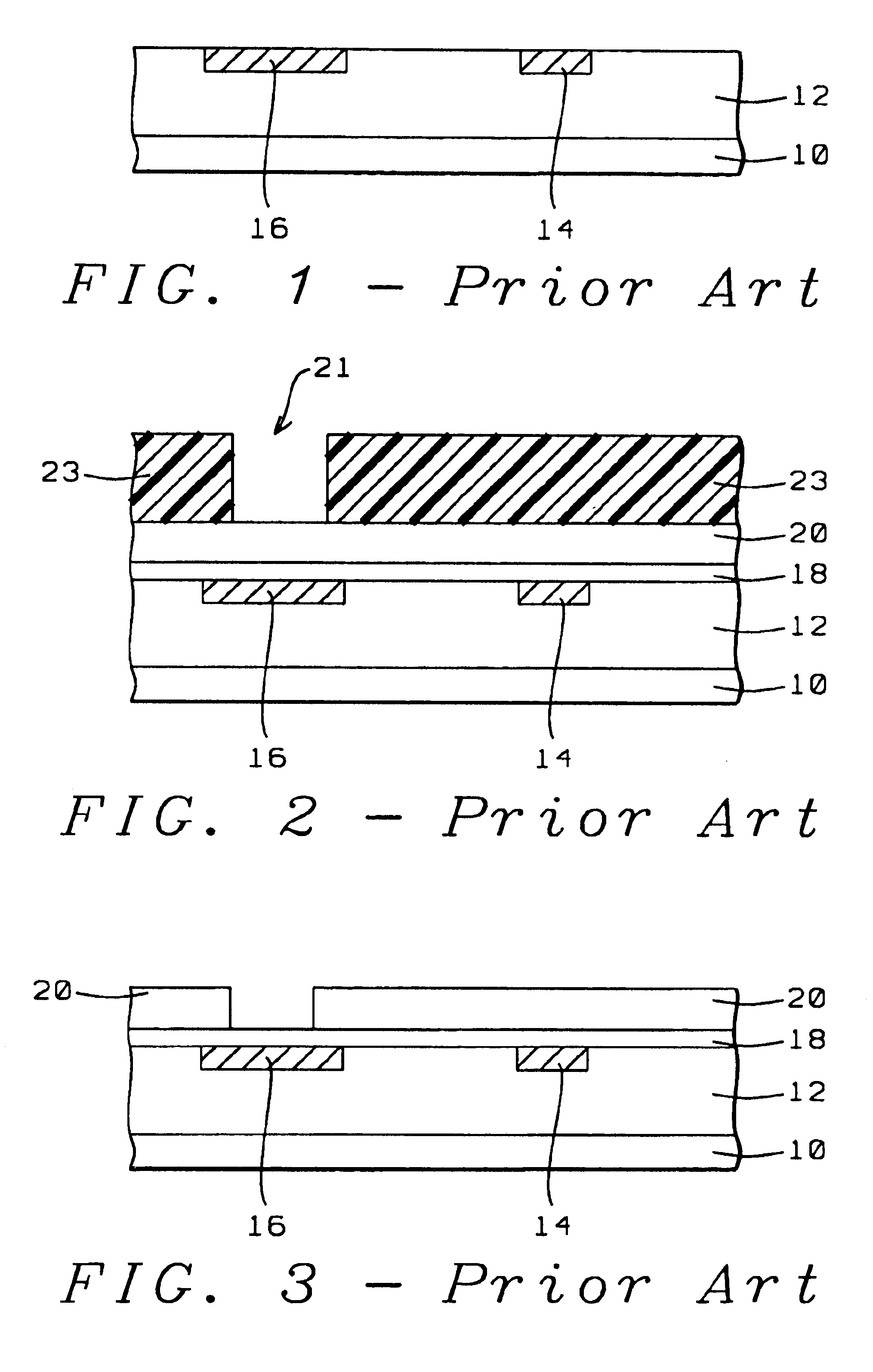
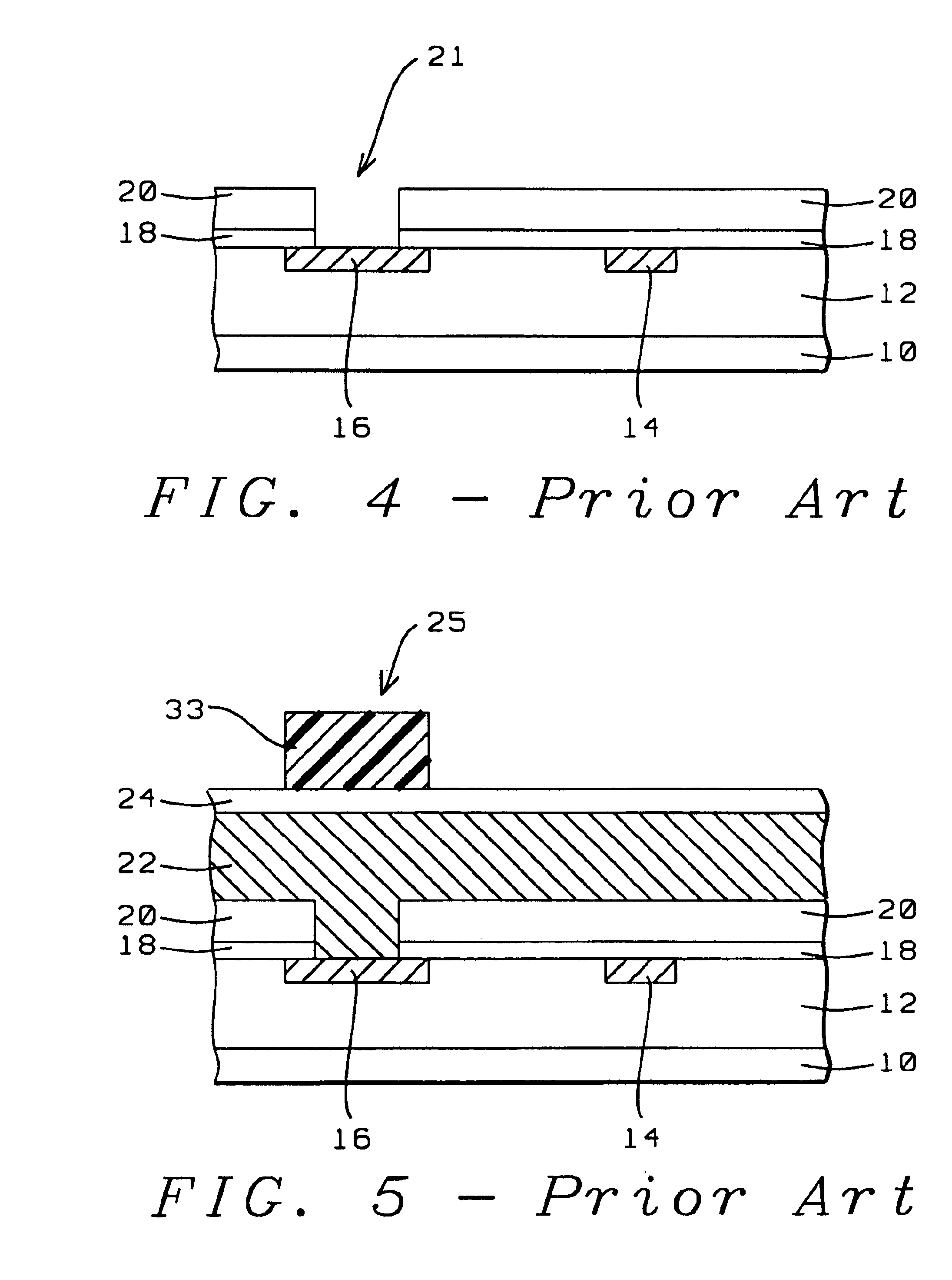
[0037]In order to enhance an understanding of the invention, a conventional method of creating a contact pad opening combined with creating a fuse opening will first be highlighted. For this purpose, FIGS. 1 through 11 will be used.

[0038]Referring now first specifically to FIG. 1, there is shown a cross section of a semiconductor surface 10, typically the surface of a monocrystalline silicon substrate, over which active semiconductor devices (not shown) have been created. Electrical access must be provided to the semiconductor devices that have been created in or over the surface of substrate 10. For this purpose, a layer 12 of conductive interconnect traces has been created whereby this layer may contain one or more overlying and interconnected layers of conductive traces, overlying layers being interconnected with the conventional contact plugs or via interconnects. The details of the interconnect layers that are assumed to be provided in layer 12 are not highlighted in the cross ...


PUM


Abstract

A new process flow is provided for the creation of a fuse contact and a bond pad. The invention starts with a semiconductor substrate over the surface of which is provided top level metal and fuse metal in the surface of a layer of insulation deposited over the surface of the substrate. A first etch stop layer is deposited over the surface of the layer of insulation over which a first passivation layer is deposited, an opening is created through these layers exposing the top level metal. A metal plug is created overlying the exposed surface of the top level metal. A stack of a patterned and etched hard mask layers, having been deposited at part of the creation of the metal plug and overlying a layer of metal plug material, remains in place over the surface of the created metal plug. A second layer of passivation material is deposited, the second layer of passivation is patterned and etched exposing the surface of the first layer of passivation overlying the fuse metal and exposing the surface of the stack of hard mask layers overlying the created metal plug. The stack of hard mask layers is then removed from the surface of the metal plug, exposing the surface of the metal plug to serve as a contact pad and further reducing the thickness of the first layer of passivation over the surface of the fuse metal, making the fuse more accessible for fuse blowing.

Description

BACKGROUND OF THE INVENTION[0001](1) Field of the Invention[0002]The invention relates to the fabrication of integrated circuit devices, and more particularly, to a method for the creation of a reliable top metal fuse.[0003](2) Description of the Prior Art[0004]Increased semiconductor device performance has over the years been achieved by decreasing device dimensions and by increasing device packaging densities. The therefrom following sharp reductions in device feature size imposes increasingly strict limitations on the technologies that are used for semiconductor device creation. Increasing device density requires the creation of more complex networks of interconnect traces over a surface in which multiple active semiconductor devices have previously been created, a requirement that is typically addressed by increasing the number of overlying layers of electrical interconnect wiring. It is in this respect not uncommon to use from two to six overlying layers of conductive interconn...

Claims


Application Information

Patent Timeline
Patent Type & Authority Patents(United States)
IPC IPC(8): H01L21/02H01L21/44H01L23/48H01L23/525
CPCH01L23/5258H01L2924/0002H01L2924/00
Inventor LEE, TZE-LIANGCHEN, CHAO-CHEN
Owner TAIWAN SEMICON MFG CO LTD
Learn More