Polishing method, polishing system and process-managing system

a polishing system and polishing technology, applied in the field of planarization during, can solve the problems of uneven surface of semiconductor devices, increased process steps in semiconductor manufacturing processes, and more complex processes, and achieve the effects of stable polishing, accurate prediction of film thickness distribution, and precise film thickness control

Inactive Publication Date: 2005-07-05
PANASONIC CORP
View PDF3 Cites 24 Cited by
  • Summary
  • Abstract
  • Description
  • Claims
  • Application Information

AI Technical Summary

Benefits of technology

[0015]According to this polishing method of the present invention, the predicted film thickness distribution and the target film thickness distribution are compared so that, before polishing of the film to be polished, the polishing time and the pressure against the polishing pad at each of the plurality of regions of the film to be polished are controlled. That is, pressure against the polishing pad at each of the plurality of regions of the film to be polished is not changed during polishing. Consequently, the equilibrium of the force acting between the polishing pad and the wafer to be polished is not upset during polishing. In addition, because the pressure against the polishing pad at each of the plurality of regions of the film to be polished is not changed during polishing, stable polishing is possible.
[0040]Also, if numerous wafers are to be polished, then the polishing rate distribution of the film to be polished that is obtained through polishing the wafer immediately prior is utilized, so that an accurate predicted film thickness distribution is always yielded for each wafer, and the pressure against the polishing pad at each of the plurality of regions of the film to be polished and the polishing time that are calculated based on the predicted film thickness distribution can also be accurately estimated. Thus, numerous wafers in which the polished film has the target film thickness distribution can be obtained.

Problems solved by technology

Recent advances in the miniaturization of semiconductors have led to an increase in the number of process steps in semiconductor manufacturing processes and have made the processes more complex.
As a result, problems caused by unevenness (steps) present in the surface of semiconductor devices (such as variation in resist dimensions when patterning with photolithography, and wiring shorts at step portions), which have conventionally not been of particular concern, are becoming noticeable.
First, with this method, if the film thickness distribution that is obtained differs from the target, then the pressure within the chamber is altered during polishing so as to draw the film thickness distribution closer to the target. At this time, the equilibrium of the force due to the relative motion acting between the polishing pad and the wafer is upset, and irregular polishing (such as a polishing rate locally above predicted values) occurs as a consequence. In the worst cases, there is a risk that the wafer may break or be detached from the carrier head, for example.
Also, during the CMP process, environmental factors such as changes in temperature during polishing may cause the polishing rate to change.
Consequently, environmental parameters being changed by altering the pressure within the chamber during polishing, as in the above method, results in an increase in the number of unstable factors when polishing.
With this method of measurement, because the wafer is rotated during polishing, it is not possible to control at what parts of an actual wafer that is provided with patterns the light beam emanated from the light source is irradiated.
Thus, the above method is not suitable when precise film thickness control is required.

Method used


Image

  • Polishing method, polishing system and process-managing system
  • Polishing method, polishing system and process-managing system
  • Polishing method, polishing system and process-managing system

Examples


embodiment 1

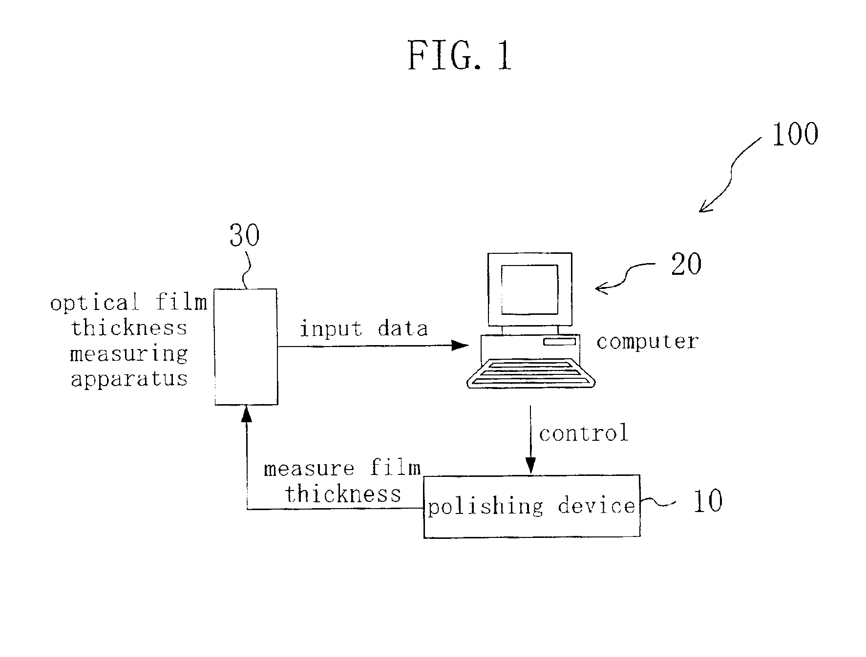
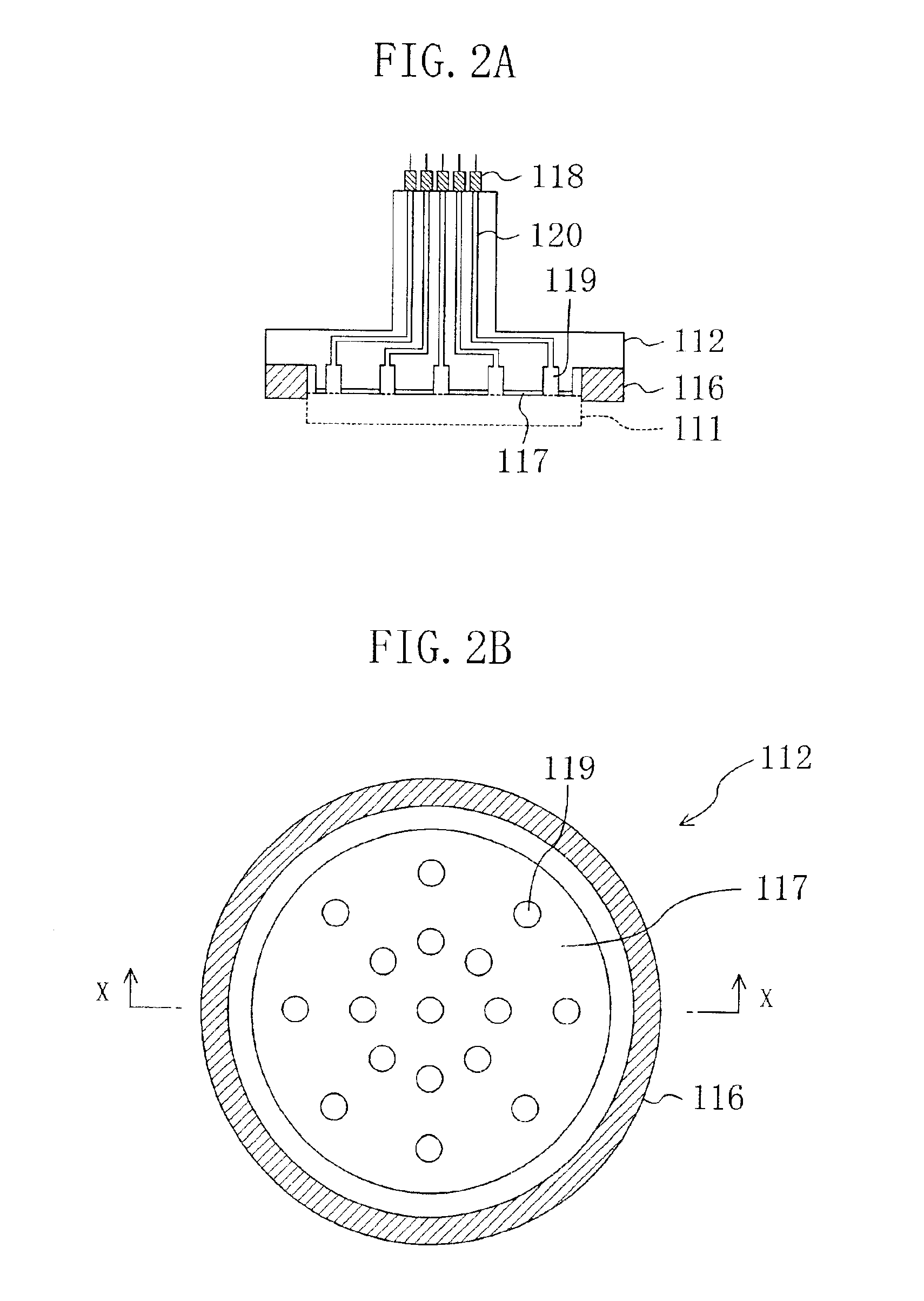
[0059]FIG. 1 schematically shows a polishing system 100 of this embodiment. FIG. 2A is a cross-sectional view of the carrier head that is employed in this embodiment, and FIG. 2B shows the bottom surface of the carrier head shown in FIG. 2A. It should be noted that FIG. 2A is a cross-sectional view taken along the X—X line shown in FIG. 2B.

[0060]As shown in FIG. 1, the polishing system 100 of this embodiment is provided with a polishing device 10, a computer 20 for controlling the polishing device 10, and an optical film thickness measuring apparatus 30.

[0061]The polishing device 10 has substantially the same configuration as the conventional polishing device 200, except that the carrier head 112 of the polishing device 10 of this embodiment is configured differently than that of the conventional example.

[0062]As shown in FIGS. 2A and 2B, the carrier head 112 is provided with a retainer ring 116, a wafer holding seal 117, a plurality of apertures provided in the bottom surface of th...

embodiment 2

[0083]In this embodiment, a specific example of the configuration of the polishing system100 of Embodiment 1 is described with reference to FIG. 6.

[0084]The polishing system 100 includes a polishing block A, in which the polishing device 10 has been provided, a measuring block B for measuring the film thickness of the film to be polished on the wafer that is polished by the polishing device 10, a control block C for controlling the polishing device 10, and a holding block D for holding wafers that need to be polished. The polishing block A is separated from the other three blocks by a wall 123 made of a transparent plastic.

[0085]The polishing device 10 that is provided in the polishing block A is the polishing device that was described in Embodiment 1.

[0086]The optical film thickness measuring apparatus 30 for measuring the film thickness of the film to be polished on the wafer that is polished by the polishing device 10 is provided in the measuring block B. The optical film thickne...

embodiment 3

[0096]In Embodiments 1 and 2, the polishing device 10 is given a configuration in which the carrier head shown in FIGS. 2A and 2B is employed to independently control, at each specific region, the force at which the wafer 111 is pressed against the polishing pad 110, but as long as the polishing device 10 has a configuration where a changeable pressure can be independently applied to a plurality of regions on the wafer 111, it can be configured differently and still achieve a similarly high degree of planarization. In this embodiment, one example of a modified polishing device is described with reference to FIG. 1.

[0097]FIG. 7A is a lateral view of the polishing device of this embodiment, and FIG. 7B is a top view of the polishing device of this embodiment.

[0098]As shown in FIGS. 7A and 7B, a polishing device 10′ of this embodiment is provided with two rollers 159, a polishing belt 160 wound around the two rollers, a carrier head 162, an air platen 163 provided in opposition to the ...


PUM


Abstract

A polishing method of the present invention is a polishing method for planarizing a film to be polished that is deposited on a wafer, and includes a step (a) of establishing a polishing rate distribution of the film to be polished that is deposited on the wafer and a target film thickness distribution after polishing of the film to be polished, a step (b) of measuring a film thickness distribution before polishing of the film to be polished, a step (c) of calculating a predicted film thickness distribution after polishing of the film to be polished from the film thickness distribution before polishing and the polishing rate distribution, a step (d) of calculating a pressure against a polishing pad for each of a plurality of regions of the film to be polished and a polishing time from the predicted film thickness distribution and the target film thickness distribution, and a step (e) of polishing while applying the pressure against the film to be polished during the polishing time.

Description

BACKGROUND OF THE INVENTION[0001]The present invention relates to polishing methods and polishing devices, and in particular relates to planarization during manufacturing processes for semiconductor devices.[0002]Recent advances in the miniaturization of semiconductors have led to an increase in the number of process steps in semiconductor manufacturing processes and have made the processes more complex. As a result, problems caused by unevenness (steps) present in the surface of semiconductor devices (such as variation in resist dimensions when patterning with photolithography, and wiring shorts at step portions), which have conventionally not been of particular concern, are becoming noticeable. Thus, in recent semiconductor manufacturing processes, a high degree of planarization of the semiconductor device surface is imperative.[0003]Chemical mechanical polishing (hereinafter abbreviated as CMP) is a widely employed polishing method for planarizing the surface of semiconductor dev...

Claims


Application Information

Patent Timeline
Patent Type & Authority Patents(United States)
IPC IPC(8): B24B49/03B24B49/02B24B49/16B24B37/04B24B41/06B24B51/00H01L21/00H01L21/02H01L21/3105
CPCB24B49/03B24B49/16B24B51/00H01L21/67253B24B37/013B24B37/042B24B37/30H01L21/31053
Inventor KAMADA, HIROYUKI
Owner PANASONIC CORP
Why Eureka
Try Eureka