Chemical-mechanical polishing equipment for semiconductor wafers

A technology for chemical machinery and wafers, applied in semiconductor/solid-state device manufacturing, metal processing equipment, grinding machine tools, etc., can solve the problems of calibration accuracy, sharp increase in shear force, workbench pollution, etc., to achieve Improve polishing accuracy, avoid air gap, and stabilize polishing effect

Active Publication Date: 2018-06-01
汉斯半导体(江苏)有限公司
View PDF6 Cites 3 Cited by
  • Summary
  • Abstract
  • Description
  • Claims
  • Application Information

AI Technical Summary

Problems solved by technology

[0004] (1) The levelness of the wafer in the initial state before it is intended to be in contact with the polishing problem, because the traditional structure generally directly raises and lowers the motor that drives the wafer to rotate. Due to the vibration of the motor during work, the state of the laser measurement is only The levelness in a certain state, so there is a problem in the accuracy of the calibration;
[0005] (2) The domestic transmission CMP polishing equipment is still transplanted to the traditional machining grinder structure. Since the precision of traditional machining is far lower than that of wafer processing, if the new structure is not redesigned, the high speed of the traditional structure will inevitably torque Low, especially when the wafer and the polishing plate are in contact, the shear force in the horizontal direction of the two end faces will suddenly increase, which will easily lead to processing errors. Often long-term experimental research, the processing error of wafer polishing is often the contact It is generated instantly, and the room for subsequent improvement through laser ranging is not very high;
[0006] (3) At this stage, the relatively mature solution to polishing accuracy is generally laser interferometry. In the existing chemical mechanical polishing method, the slurry is still directly flushed. In the initial stage of polishing, between the polishing plate and the wafer surface It is easy to generate air gaps, mixed with slurry and waste debris, and a stable turbulent layer will also be formed as the polishing progresses, which will interfere with the vibration of the spectral signal and affect the monitoring effect. When the wafer size is larger, this The more obvious the interference will be;
[0007] (4) Slurry recovery during grinding has been a problem for a long time. If it is not recovered in time, the pollution of the workbench will also affect the subsequent processing.

Method used


Image

  • Chemical-mechanical polishing equipment for semiconductor wafers
  • Chemical-mechanical polishing equipment for semiconductor wafers
  • Chemical-mechanical polishing equipment for semiconductor wafers

Examples


Embodiment 1

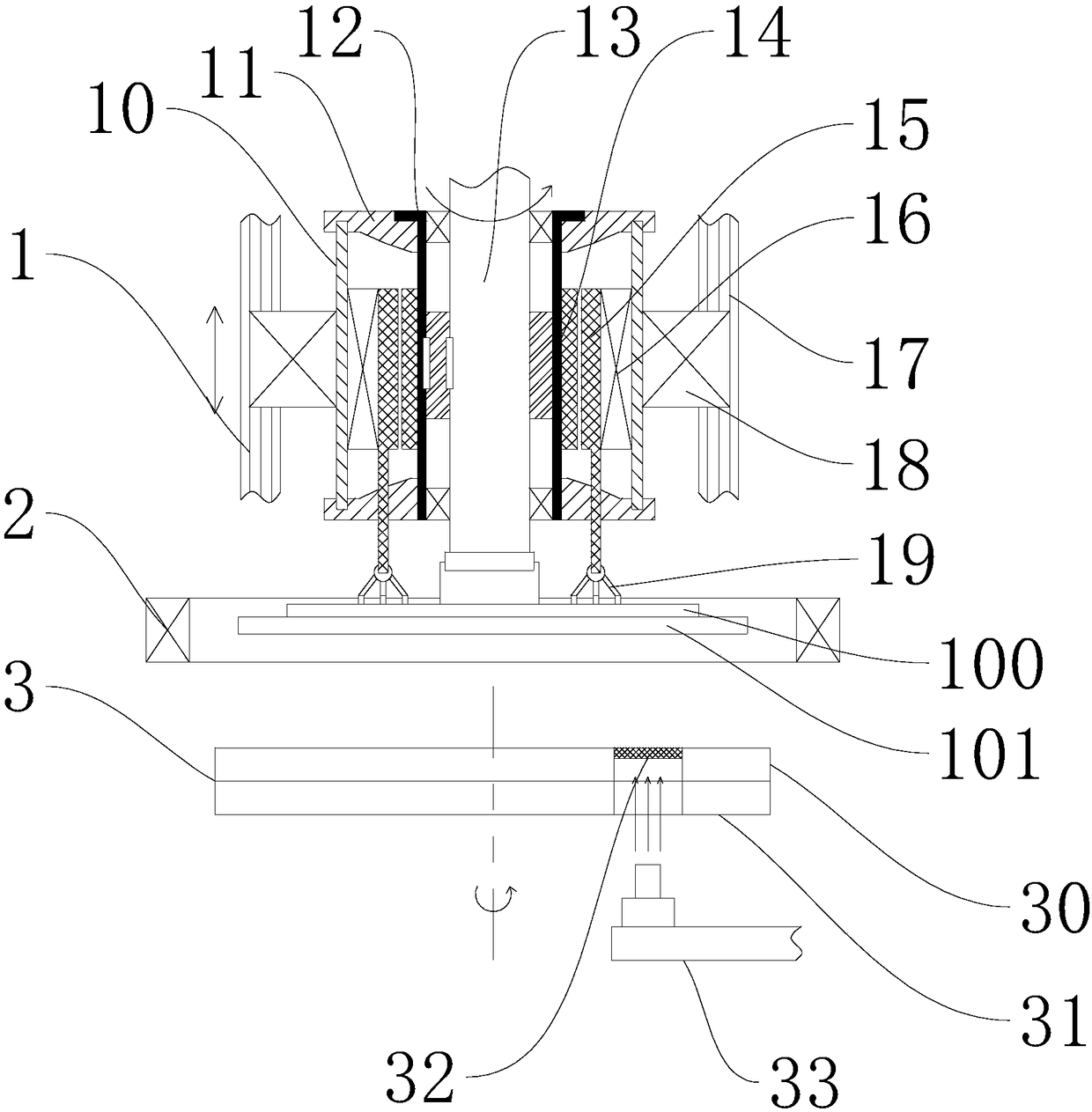
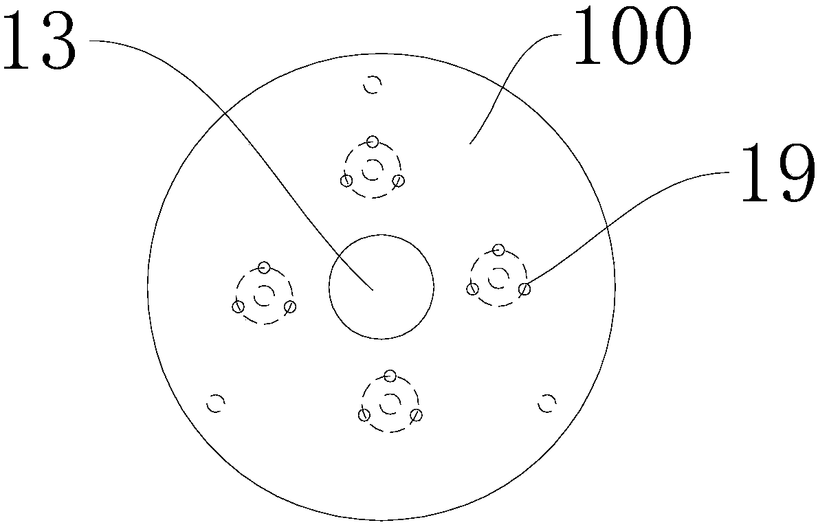
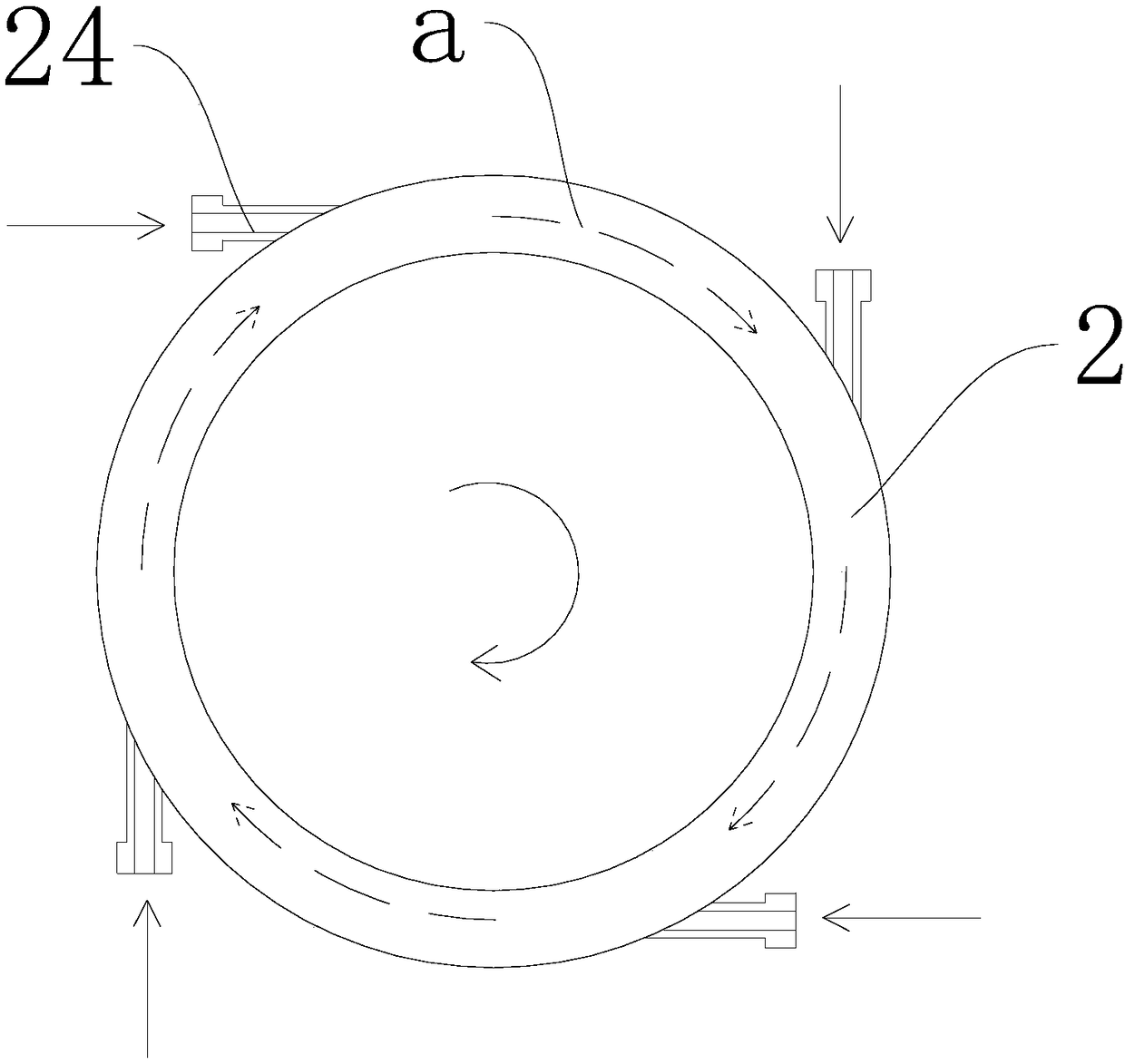
[0031] Such as Figure 1 to Figure 4 The shown embodiment 1 of a chemical mechanical polishing equipment for semiconductor wafers of the present invention includes a wafer clamping assembly 1, a polishing slurry control device 2, and a CMP device 3 arranged sequentially from top to bottom,

[0032] The wafer clamping assembly 1 has a hollow mounting cylinder 10 with openings at both ends. Sealing end caps 11 are provided on the upper and lower ends of the mounting cylinder 10. Between the two sealing end caps 11 are rotatably connected Spacer 12, drive motor rotating shaft 13 is installed through the bearing in the inner chamber of spacer 12, is provided with driving gear ring 14 on the outer wall of spacer 12, is provided with driven gear ring 15 meshing with driving gear ring 14, ingenious The spacer 12 and the annular chamber between the inner wall of the installation cylinder 10 are used to transmit the power of the drive motor shaft 13, while ensuring the synchronous spee...


PUM


Abstract

The invention relates to chemical-mechanical polishing equipment for semiconductor wafers. The equipment comprises a wafer clamping assembly, a grinding pulp control device and a CMP device arranged in sequence from top to bottom. The equipment is simple in structure, discards a traditional grinding machine structure, and dose not directly control lifting of a main shaft of a motor which controlsrotation of the wafers; a mounting cylinder is provided; a wafer levelness checking device and the main shaft of the motor are linked and arranged in the mounting cylinder together; a single linear drive of the mounting cylinder is directly lifted, so that the precision is higher, the vibration problem of the motor is isolated, and the engagement problem at the contact moment can be solved; and meanwhile, the grinding pulp control device forms homogenous annular water film layers between the wafers and polishing plates, so that the air gap problem can be prevented, the polishing process can bestabilized, the laser interference monitoring is convenient, and the polishing precision is improved.

Description

technical field [0001] The invention relates to the technical field of semiconductor wafer manufacturing, in particular to chemical mechanical polishing equipment for semiconductor wafers. Background technique [0002] In the well-known technical field, chemical mechanical polishing is a step in the semiconductor process, referred to as CMP. This technology was introduced into the semiconductor silicon wafer process in the early 1990s. Chemical mechanical polishing has been proven to be the best and only one that can achieve global planarization. Technology. In the semiconductor manufacturing process, various layers of circuits are superimposed and integrated on the surface of the wafer through the previous process. During the manufacturing process, the surface will inevitably be irregular. Failure of circular circuits. [0003] In the traditional CMP process, similar to the general polishing process, the wafer is in contact with the polishing plate, through the transmissi...

Claims


Application Information

Patent Timeline
Patent Type & Authority Applications(China)
IPC IPC(8): B24B37/00B24B37/005B24B37/34H01L21/67
Inventor 曹云娟
Owner 汉斯半导体(江苏)有限公司
Why Eureka
Try Eureka