Semiconductor integrated circuit and memory test method

a technology of integrated circuits and memory, applied in the field of semiconductor integrated circuits, can solve the problems of increasing the area of the bist circuit, the difficulty of achieving a bist circuit, so as to achieve the effect of raising the quality of the test pattern

Inactive Publication Date: 2005-07-12
SOCIONEXT INC
View PDF14 Cites 35 Cited by
  • Summary
  • Abstract
  • Description
  • Claims
  • Application Information

AI Technical Summary

Benefits of technology

[0057]With these configurations, the clock selection section selects either the second clock or the inverted clock of the second clock, and the test data selection section selects either the first or second test data depending on the selected clock. By reversing the state of the selection by the clock selection section, the timing for selecting the first and second test data can be reversed. As a result, the quality of a test pattern can be raised. In addition, when an address signal is supplied as a test pattern, the increment and decrement of the address signal can be carried out selectively. The other effects are similar to those of the first, second sixth or seventh invention.

Problems solved by technology

However, since the operation frequency of the memory is very high, it is difficult to attain a BIST circuit capable of operating at such a high operation frequency, thereby causing a problem of attaining such a BIST circuit.
In addition, cells having high drive capability are required for high-speed operation, thereby causing a problem of increasing the area of the BIST circuit.
Furthermore, the clock frequency of the BIST circuit is required to be raised for high-speed operation, thereby causing a problem of increasing the power consumption of the BIST circuit.

Method used


Image

  • Semiconductor integrated circuit and memory test method
  • Semiconductor integrated circuit and memory test method
  • Semiconductor integrated circuit and memory test method

Examples


first embodiment

(First Embodiment)

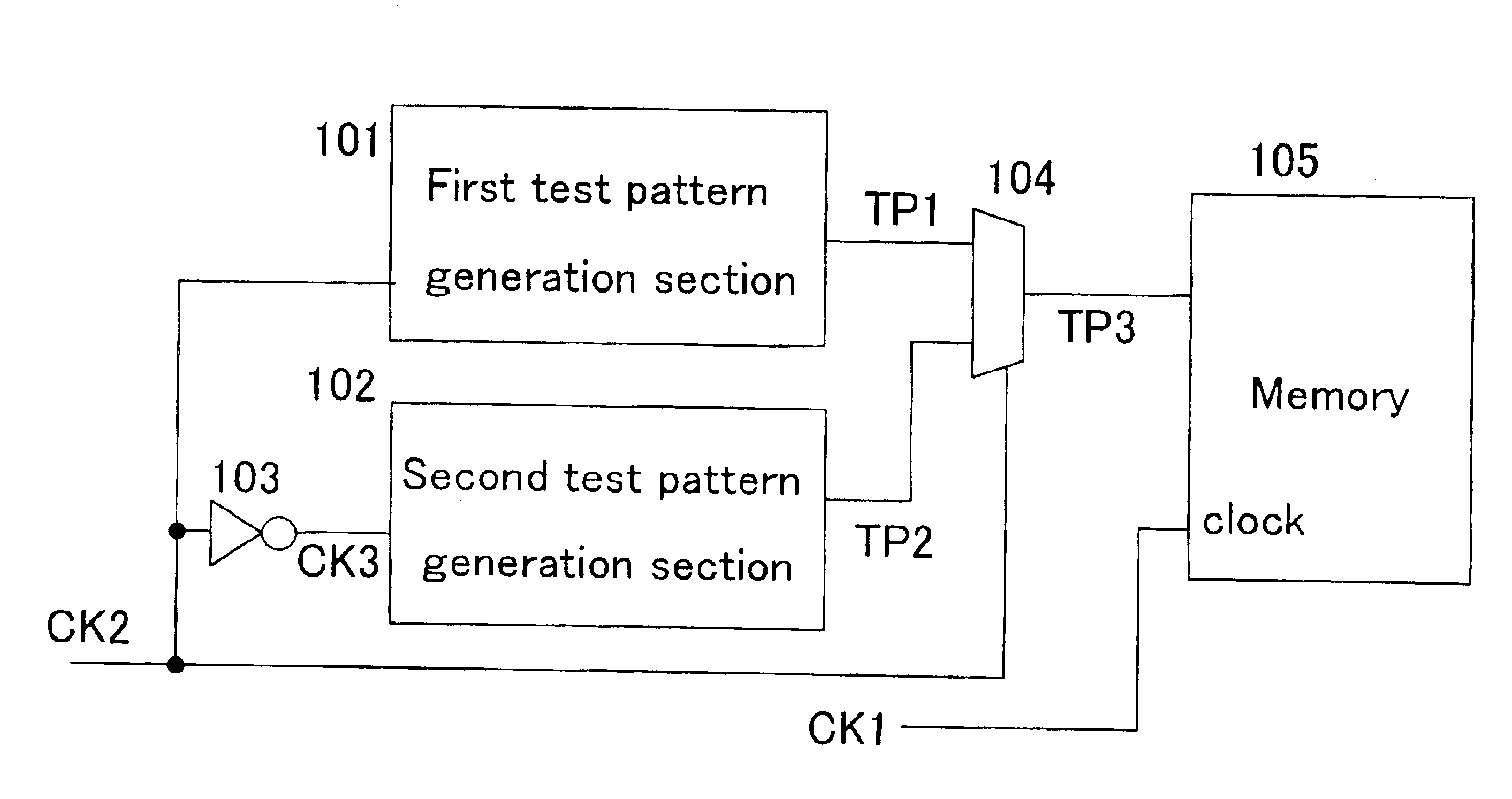
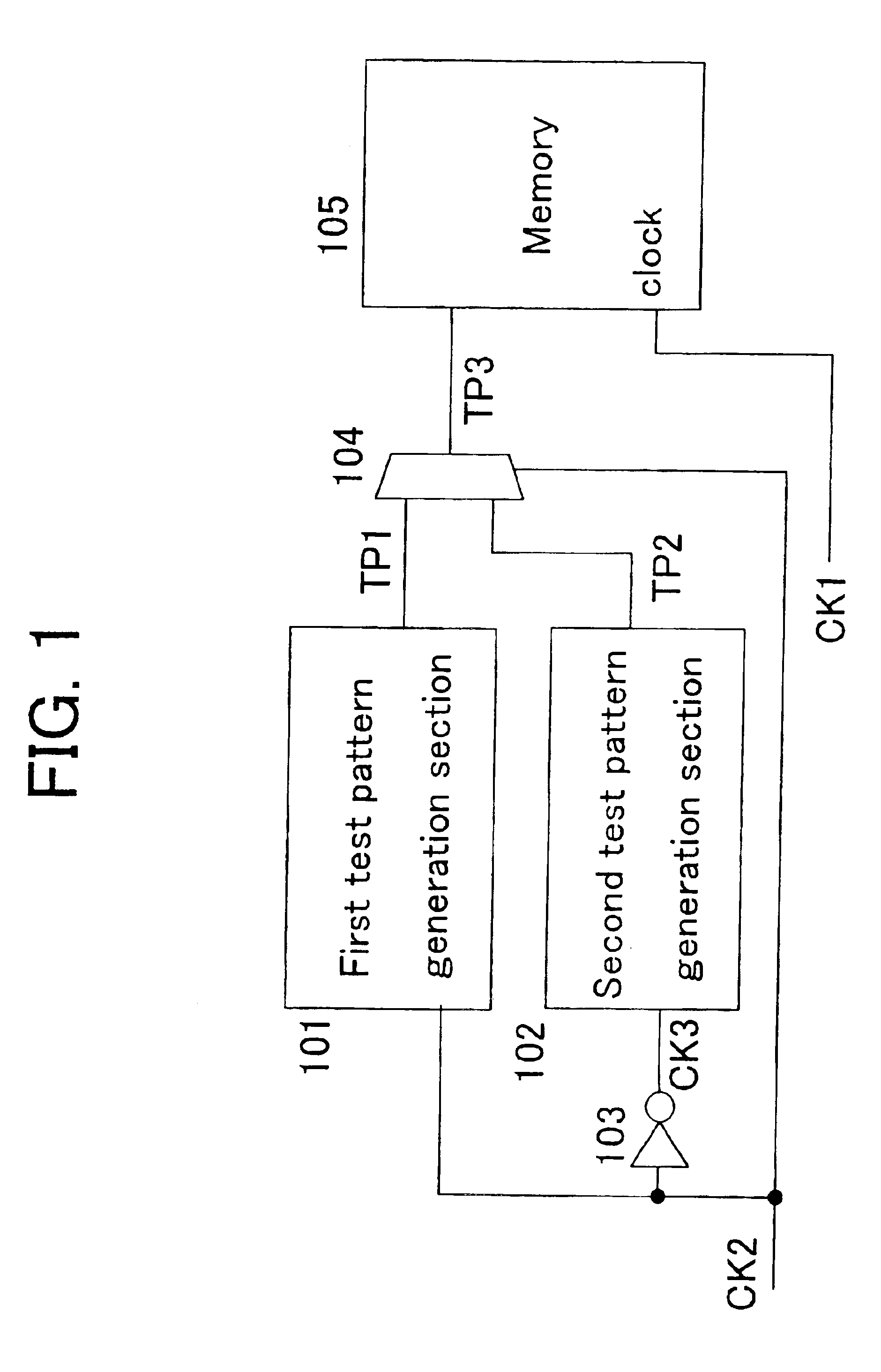
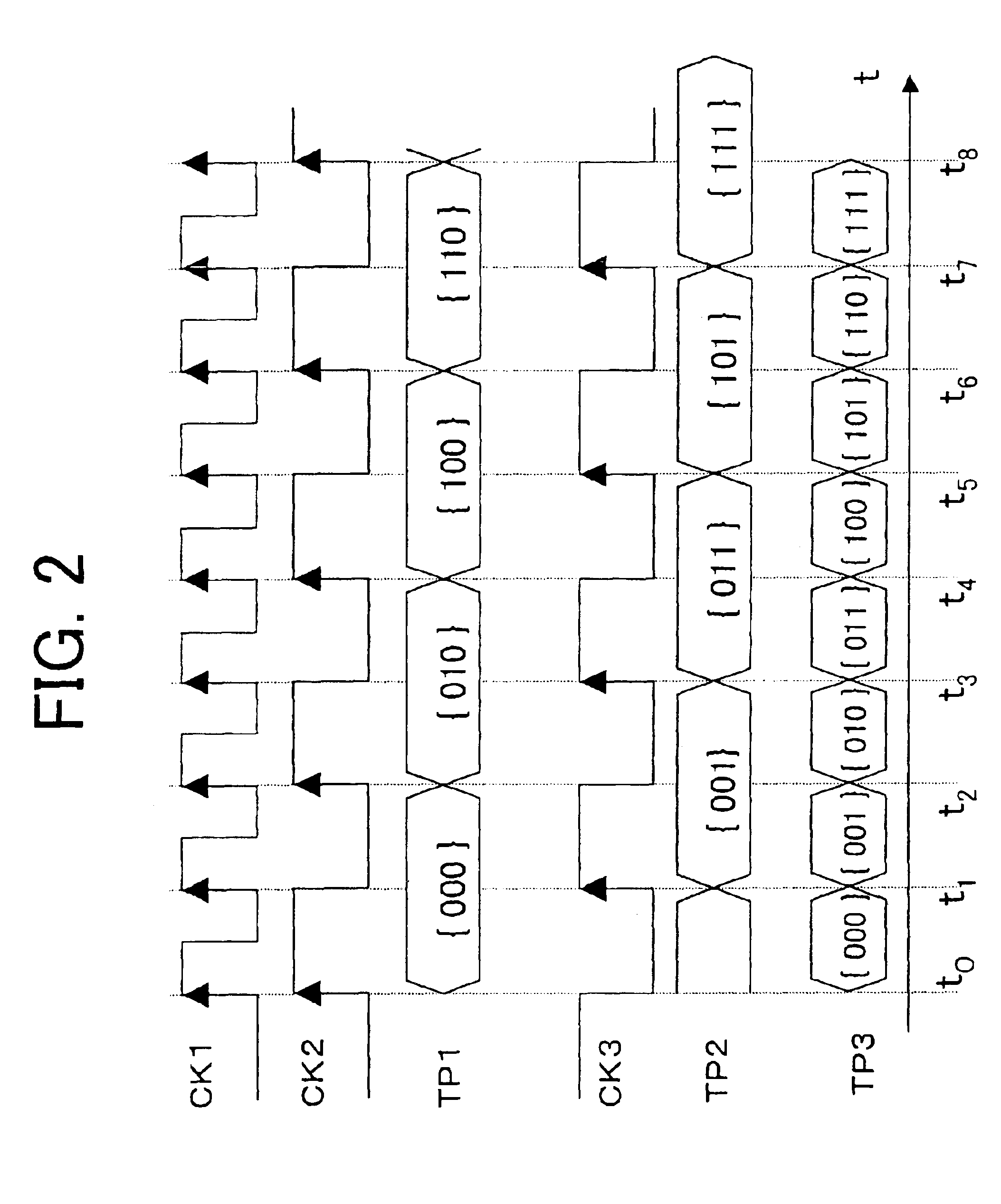
[0087]FIG. 1 is a block diagram illustrating a semiconductor integrated circuit and a memory test method in accordance with a first embodiment of the present invention, and FIG. 2 is a timing chart at various sections of FIG. 1.

[0088]In FIG. 1, numeral 101 designates a first test pattern generation section operating in synchronization with the rising edge of an input clock. Numeral 102 designates a second test pattern generation section operating in synchronization with the rising edge of an input clock. Numeral 103 designates an inverter for generating an inverted clock. Numeral 104 designates a test data selection section. These constitute a BIST circuit. Numeral 105 designates an ordinary data rate memory to be subjected to a BIST, and the memory operates in synchronization with the rising edge of an input clock.

[0089]A first clock CK1 is a clock signal supplied to the memory 105. A second clock CK2 is a clock signal supplied to the first test pattern generation...

second embodiment

(Second Embodiment)

[0097]FIG. 4 is a block diagram illustrating a semiconductor integrated circuit and a memory test method in accordance with a second embodiment of the present invention, and FIG. 5 is a timing chart.

[0098]The memory test method using the semiconductor integrated circuit shown in FIG. 4 will be described below on the basis of a flowchart shown in FIG. 7.

[0099]In FIG. 4, numeral 201 designates a test pattern generation section operating in synchronization with the rising edge of an input clock. Numeral 202 designates an LSB0 processing section, numeral 203 designates an LSB1 processing section, and numeral 204 designates a test data selection section. These constitute a BIST circuit. Numeral 205 designates an ordinary data rate memory to be subjected to a BIST, and the memory operates in synchronization with the rising edge of an input clock.

[0100]A first clock CK1 is a clock signal supplied to the memory 205. A second clock CK2 is a clock signal supplied to the tes...

third embodiment

(Third Embodiment)

[0117]FIG. 8 is a block diagram illustrating a semiconductor integrated circuit and a memory test method in accordance with a third embodiment of the present invention, and FIG. 9 is a timing chart.

[0118]The memory test method in the semiconductor integrated circuit shown in FIG. 8 will be described below on the basis of th flowchart of FIG. 7.

[0119]The semiconductor integrated circuit differs from the semiconductor integrated circuit shown in FIG. 4 in that the circuit is equipped with a delay circuit 206 for generating a delay clock CK2′ obtained by delaying the second clock CK2. This delay circuit 206 is formed of, for example, a circuit for generating a constant delay time by arranging buffers or inverters in series or a delay device capable of generating the constant delay time.

[0120]The test data selection processing step ST303 and the test pattern application processing step ST304 in this embodiment will be described below.

[0121]At the test data selection pr...


PUM


Abstract

The present invention provides a semiconductor integrated circuit capable of testing a high-speed memory at the actual operation speed of the memory even when the operation speed of the BIST circuit of the integrated circuit is restricted.
In order to test a memory operating on a first clock, the integrated circuit is provided with a first test pattern generation section, operating on a second clock, for generating test data, and a second test pattern generation section, operating on a third clock, the inverted clock of the second clock, for generating test data. Furthermore, the integrated circuit is provided with a test data selection section for selectively outputting either the test data output from the first test pattern generation section or the test data output from the second test pattern generation section depending on the signal value of the second clock, thereby inputting the test data to the memory as test data. The frequency of the second clock is half the frequency of the first clock.

Description

BACKGROUND OF THE INVENTION[0001]1. Field of the Invention[0002]The present invention relates to a semiconductor integrated circuit capable of testing a memory by carrying out a built-in self-test, and more particularly to a semiconductor integrated circuit capable of testing a memory operating at high speed. The present invention also relates to a memory test method.[0003]2. Prior Art[0004]In recent years, as the LSI technology progresses, the operation speeds of memories included in semiconductor integrated circuits have become increasing. In order to test these memories, a built-in self-test (the so-called BIST) is generally used.[0005]FIG. 21 shows a circuit block for carrying out a BIST. In FIG. 21, numeral 401 designates a BIST circuit, and numeral 402 designates a memory to be subjected to a BIST. A first clock (memory clock) is input to the memory 402, and a second clock (BIST clock) is input to the BIST circuit 401. The memory 402 is classified into an ordinary data rate me...

Claims


Application Information

Patent Timeline
Patent Type & Authority Patents(United States)
IPC IPC(8): G11C29/04G11C29/36
CPCG11C29/12015G11C29/36G11C2029/3602
Inventor ICHIKAWA, OSAMU
Owner SOCIONEXT INC
Why Eureka
Try Eureka