Polishing apparatus

a technology of polishing apparatus and turning table, which is applied in the direction of lapping machines, manufacturing tools, and abrasive surface conditioning devices, etc., can solve the problems of existing polishing apparatus, idle time of turntables, and inability to use, and achieve the effect of compact and economical apparatus

Inactive Publication Date: 2005-07-19
EBARA CORP
View PDF23 Cites 9 Cited by
  • Summary
  • Abstract
  • Description
  • Claims
  • Application Information

AI Technical Summary

Benefits of technology

[0026]Another aspect of the invention is a polishing apparatus for polishing a circular workpiece attached to a holder device, by rotating and pressing a workpiece surface against a rotating polishing surface of a polishing table, wherein a radius of the polishing surface is smaller than a diameter but larger than a radius

Problems solved by technology

One of the problems in the existing polishing apparatus is its productivity.
This is time-consuming, resulting in idle time for the turntable 109.
Furthermore, in the existing polishing apparatus, a high relative speed between the turntable 109 and the top ring 113 is used to achieve effective polishing as well as high flatness of the wafer surface, but this high relative speed may also cause micro-scratch marks on the wafers due to abrasive particles contained in the polishing solution.
However, as mentioned above, the large size of the turntable 109 occup

Method used


Image

  • Polishing apparatus
  • Polishing apparatus
  • Polishing apparatus

Examples


Embodiment Construction

[0041]In the following, preferred embodiments will be presented with reference to the drawings.

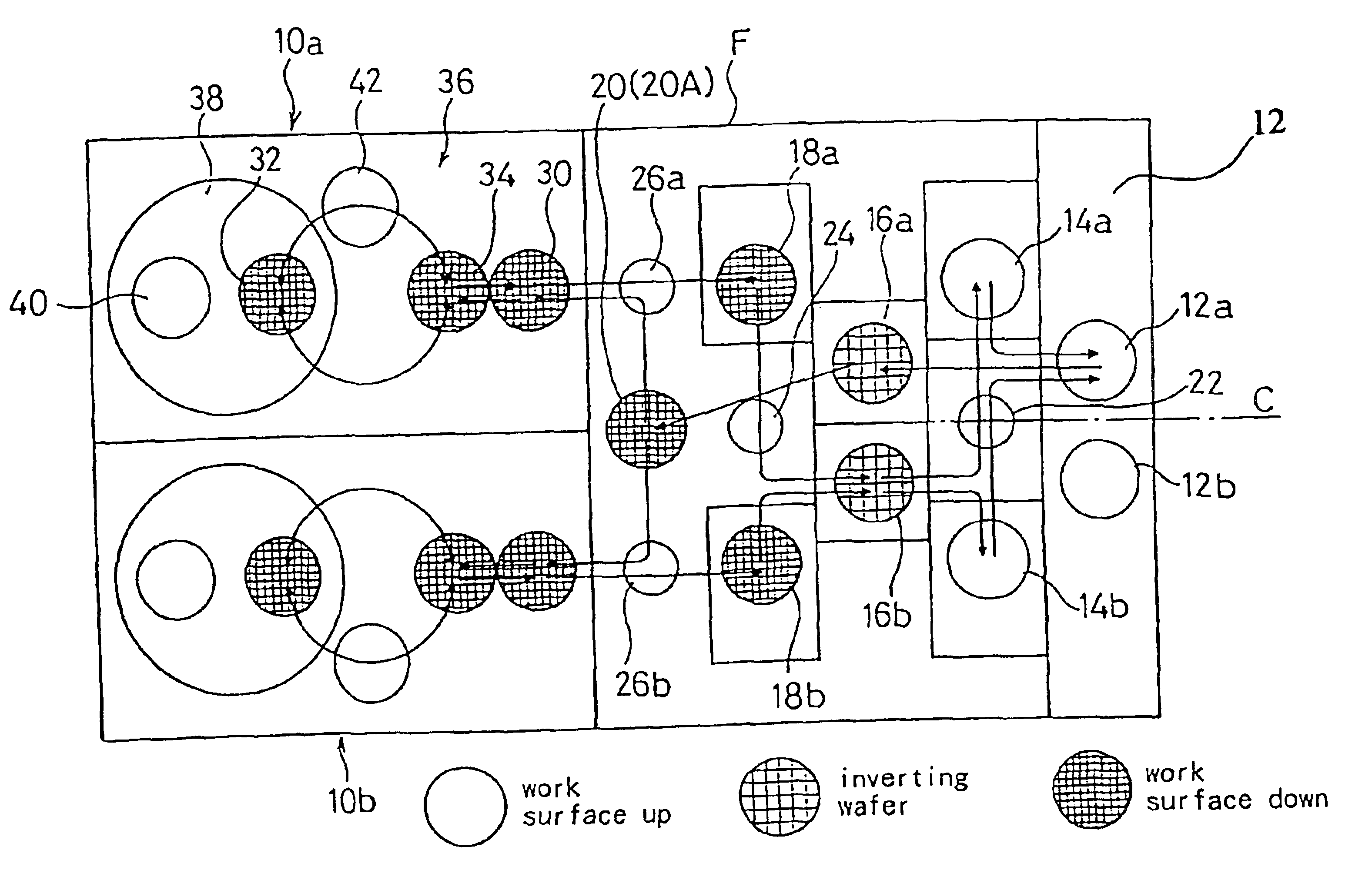
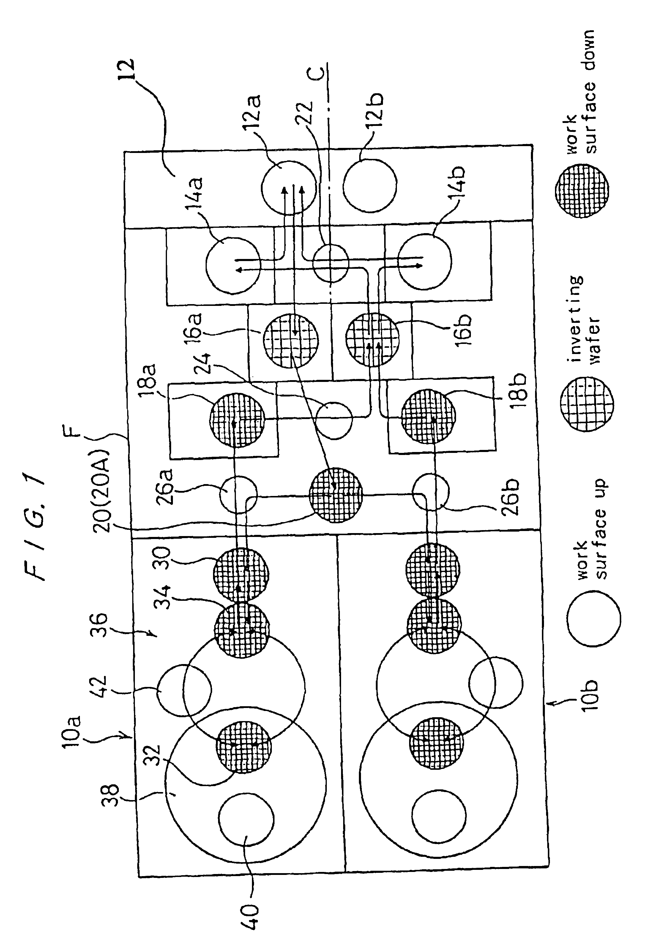
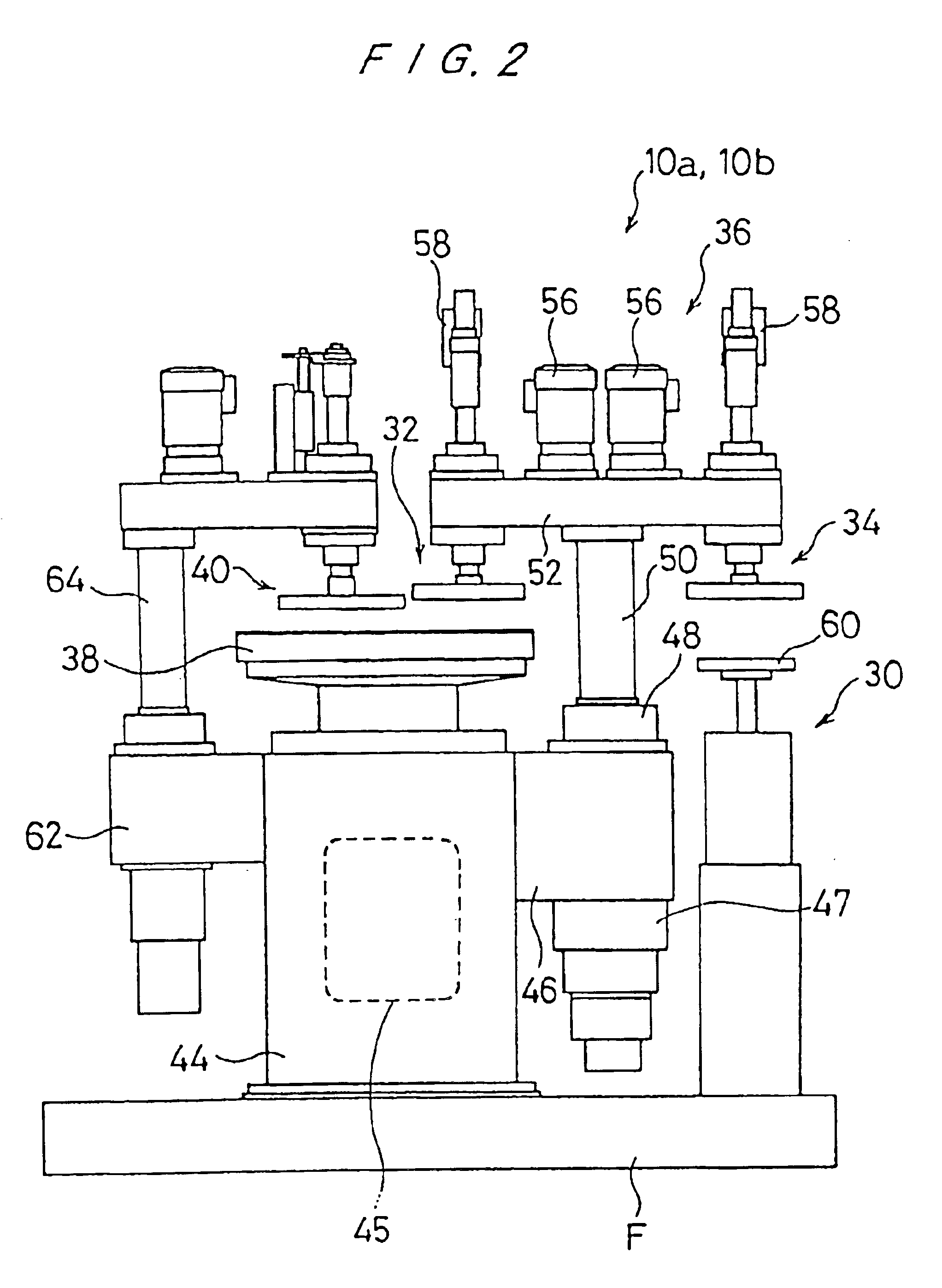
[0042]FIG. 1 is a schematic illustration of a first embodiment of the present polishing apparatus. The present polishing apparatus is contained in a rectangular-shaped floor space F, and the constituting elements arranged on the left / right sides are disposed in a symmetrical pattern with respect the center line C. Specifically, at one end of the rectangular-shaped floor, a pair of polishing units 10a, 10b are disposed symmetrically on the left and right side, respectively, and a loading / unloading unit 12 mounting a pair of cassettes 12a, 12b for storing wafers are disposed on an opposite end of the floor. Between these two ends, there are disposed, beginning from the loading / unloading unit side, a pair of secondary cleaning units 14a, 14b, a pair of wafer inverters 16a, 16b, a pair of primary cleaning units 18a, 18b, and one temporary storage station 20. The pairs of primary and secondary ...


PUM


Abstract

This invention pertains to a polishing apparatus for polishing a semiconductor wafer. The apparatus comprises a storage section that is capable of receiving a workpiece to be polished and a polished workpiece. The polishing unit that polishes the workpiece includes a primary polishing table and a secondary polishing table, wherein the polishing surface of the secondary polishing table is constructed to be arranged such that at least a portion of a surface of the workpiece being polished by the polishing surface of the secondary polishing table extends beyond an edge of the polishing surface of the secondary polishing table. Also provided is a film thickness measuring device, which measures the thickness of a film formed on a polished workpiece while the polished workpiece is held by a top ring above a pusher.

Description

[0001]This application is a divisional of U.S. application Ser. No. 09 / 984,433, filed Oct. 30, 2001, now U.S. Pat. No. 6,413,146, which is a divisional application of U.S. application Ser. No. 09 / 341,882, filed Sep. 8, 1999, now U.S. Pat. No. 6,332,826, which is a 371 of PCT / JP98 / 05252, filed Nov. 20, 1998.TECHNICAL FIELD[0002]The present invention relates to polishing apparatus in general, and relates in particular to a polishing apparatus to produce a flat and mirror polished surface on workpieces such as semiconductor wafers.BACKGROUND ART[0003]With increasing intensity of circuit integration in semiconductor devices in recent years, circuit lines have become finer and interline spacing has also been drastically reduced. With this trend for finer resolution in circuit fabrication, it is now necessary to provide a precision flat substrate surface because of the extreme shallow depth of focus required in optical photolithography using stepper reproduction of circuit layout. One met...

Claims


Application Information

Patent Timeline
IPC IPC(8): B24B27/00B24B37/04B24B53/007B24B49/12B24B1/00B24B37/10B24B37/11B24B37/27B24B37/34B24B53/017
CPCB24B27/0023B24B37/10B24B37/11B24B49/12B24B53/017B24B37/345Y10T29/53961B24B37/30B24B49/045
Inventor KATSUOKA, SEIJITSUJIMURA, MANABUSAKURAI, KUNIHIKOOSAWA, HIROYUKI
Owner EBARA CORP
Why Eureka
Try Eureka