

Silicon on insulator (SOI) transistor and methods of fabrication
a technology of silicon on insulator and transistor, applied in the direction of transistor, semiconductor device, electrical apparatus, etc., can solve the problems of inability to form thin, less than 100 nm uniform epitaxial silicon body film, present techniques are inability to fabricate fully depleted soi transistors
- Summary
- Abstract
- Description
- Claims
- Application Information
AI Technical Summary
Benefits of technology
Problems solved by technology
Method used
Image

Examples
Embodiment Construction
[0011]The present invention is a novel silicon on insulator (SOI) transistor and its method of fabrication. In the following detailed description, numerous specific details are set forth in order to provide a thorough understanding of the present invention. In other instances, well-known semiconductor processing techniques have not been described in particular detail in order to not unnecessarily obscure the present invention.
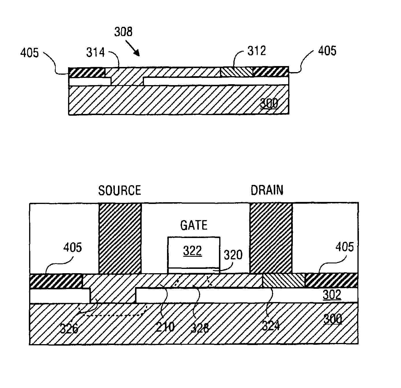
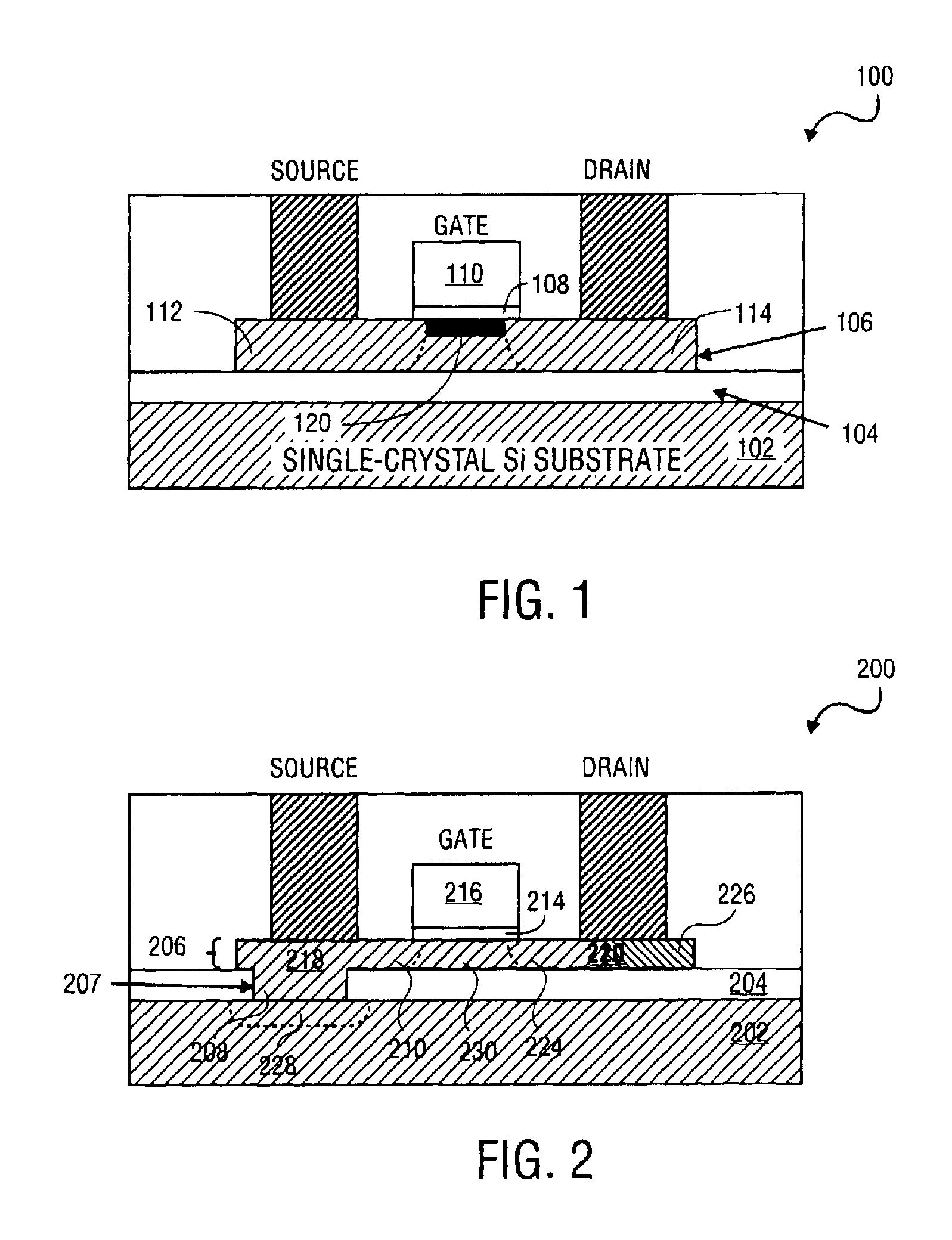
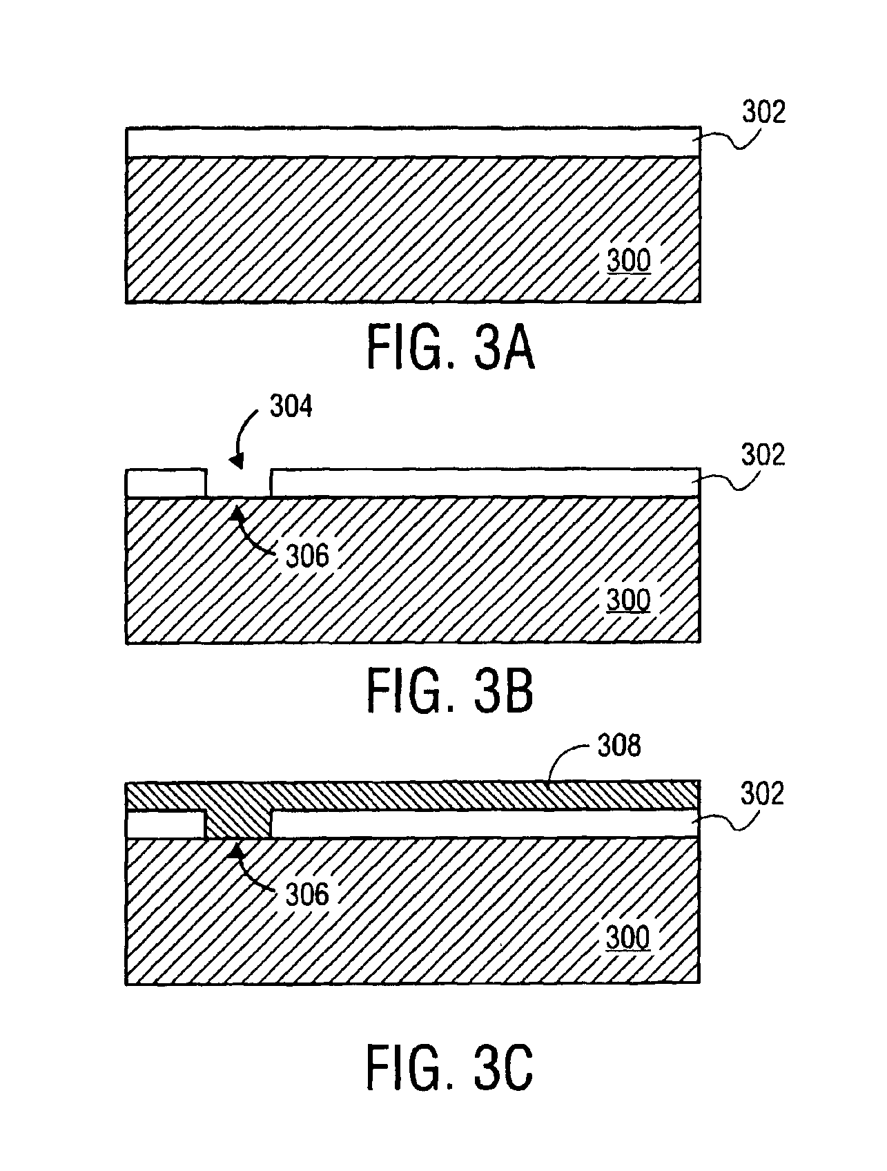
[0012]The present invention is a novel SOI transistor and its method of fabrication. The SOI transistor is fabricated utilizing the lateral crystallization of a thin deposited amorphous or polycrystalline silicon or silicon alloy that contacts a single crystalline silicon substrate through a small seed window in the insulating layer. The process of the present invention can be used to form very thin (less than 30 nanometers) and uniform thickness single crystalline silicon films for the body of the transistor enabling fully depleted SOI transistors to be fabric...
PUM
| Property | Measurement | Unit |
|---|---|---|
| length | aaaaa | aaaaa |
| thickness | aaaaa | aaaaa |
| length | aaaaa | aaaaa |
Abstract
Description
Claims
Application Information