
Permanently on transistor implemented using a double polysilicon layer CMOS process with buried contact

a polysilicon layer and permanent transistor technology, applied in the direction of semiconductor devices, semiconductor/solid-state device details, electrical equipment, etc., can solve the problems of high cost, many man-hours of highly skilled professionals, and the effect of integrating circuits

Inactive Publication Date: 2005-07-19
HRL LAB
View PDF136 Cites 20 Cited by
  • Summary
  • Abstract
  • Description
  • Claims
  • Application Information

AI Technical Summary

Benefits of technology

[0012]Designing a circuit to appear as one function, but operate as another, is a good way to protect a circuit agai

Problems solved by technology

Efforts to be able to achieve such understanding and establish successful design, development and production manufacturing of such integrated circuits involve many man-hours of highly skilled professionals and considerable expense.
However, integrated circuits protected with the art taught and referenced above look different from standard integrated circuits produced with the same CMOS process.

Method used


Image

  • Permanently on transistor implemented using a double polysilicon layer CMOS process with buried contact
  • Permanently on transistor implemented using a double polysilicon layer CMOS process with buried contact
  • Permanently on transistor implemented using a double polysilicon layer CMOS process with buried contact

Examples


Embodiment Construction

[0029]Reference will be now made to the drawings that are shown for the purpose of describing the preferred embodiment of the invention and not for limiting same.

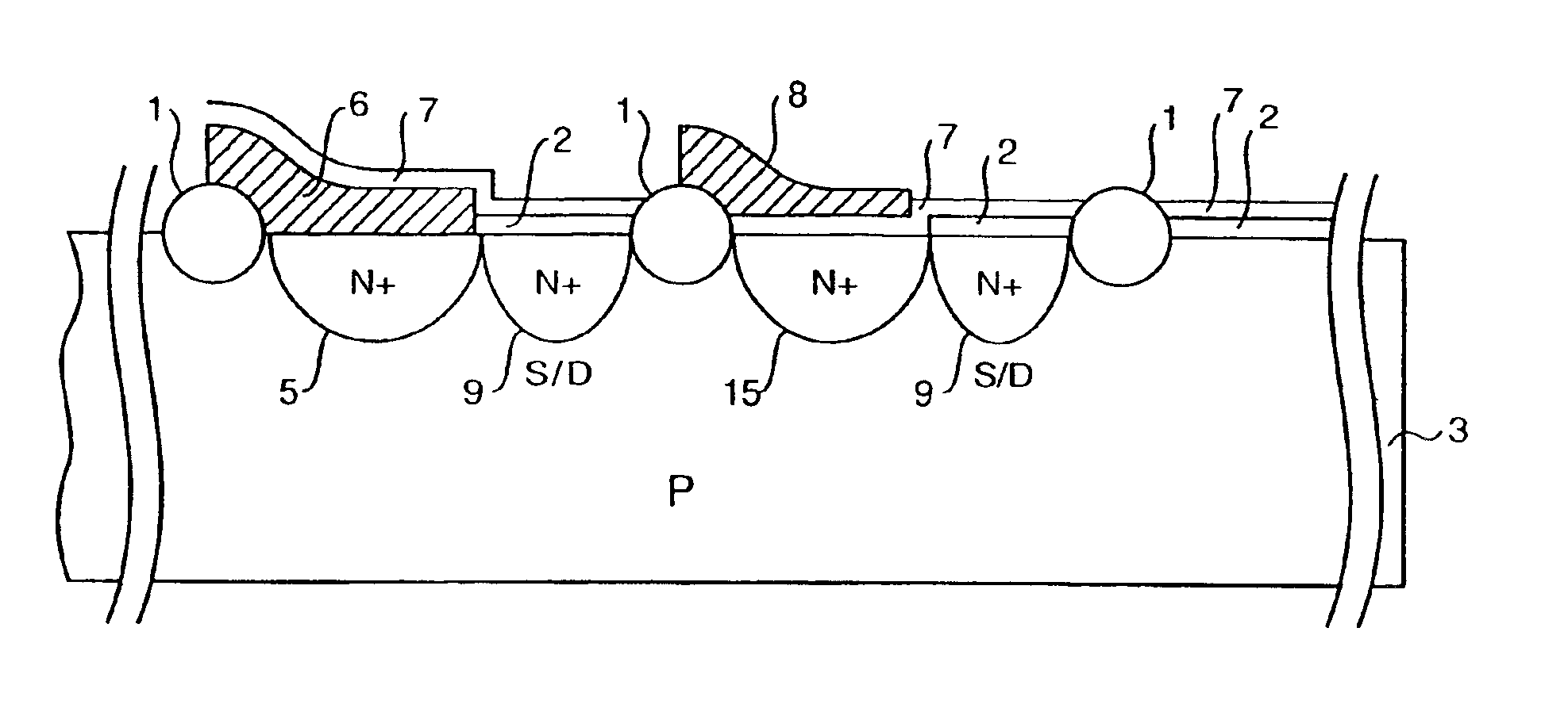
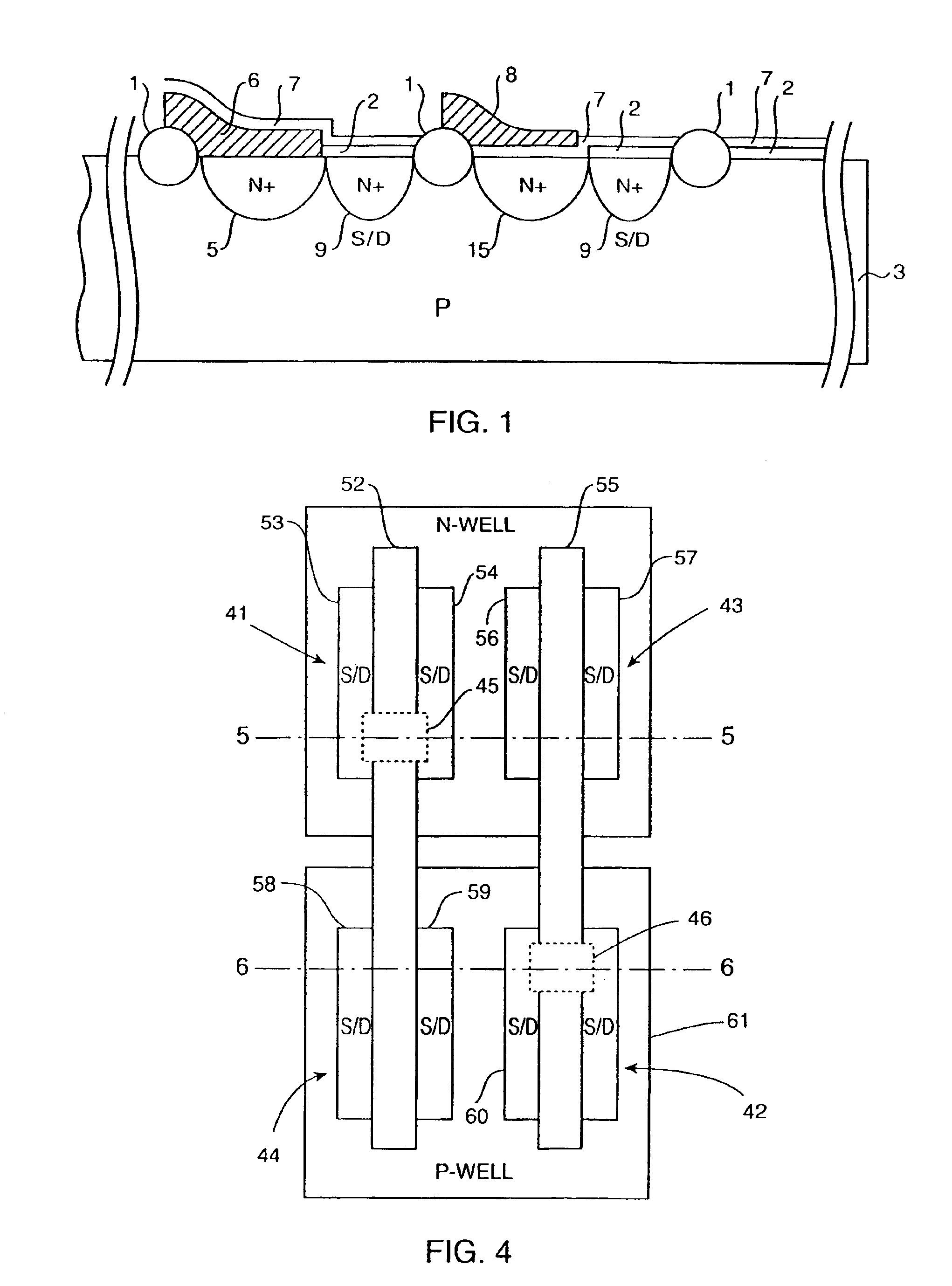
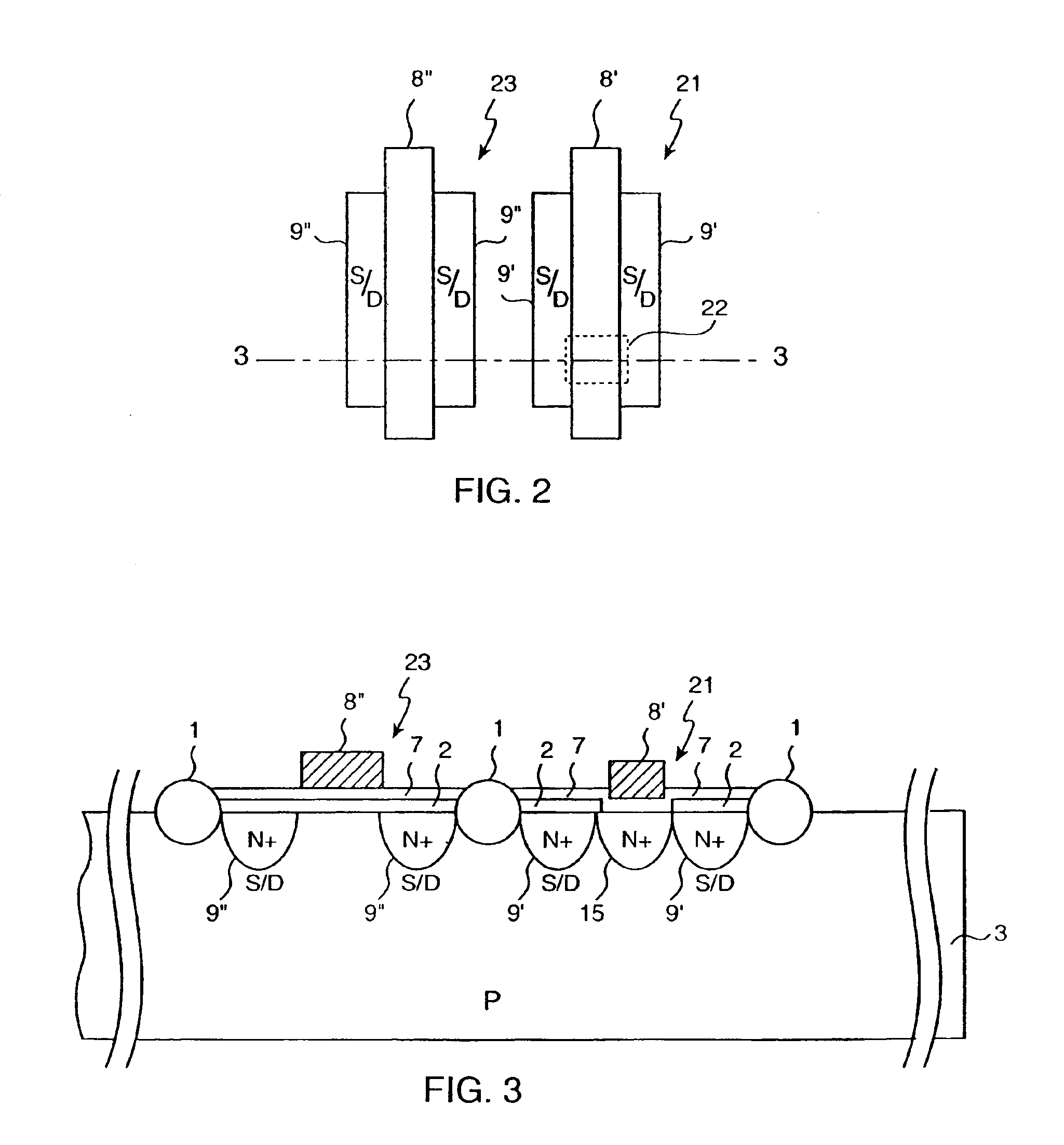
[0030]In the following FIGS. 1 to 3 the N-type buried contacts are shown, i.e. a P-well silicon region having N+ type buried contact implants and N+ type source / drain active regions. Similarly, P-type buried connections will require P+ type source / drain connections and P+ type buried contact implants.

[0031]In a double polysilicon CMOS process with buried contact, the buried contact is usually opened with masking and doped with the appropriate (i.e. N+ or P+ depending on the type of transistor) implant after the first gate oxide growth. A first layer of polysilicon is deposited to make connection to the source and drain area in the buried contact. The first layer of polysilicon can also be used to form the gate of the transistor with the first gate oxide.

[0032]In an EEPROM circuit, the first layer of polysilicon is used as t...


PUM


Abstract

A permanently-ON MOS transistor comprises silicon source and drain regions of a first conductivity type in a silicon well region of a second conductivity type. A silicon contact region of the first conductivity types is buried in the well region, said contact region contacting said source region and said drain region. A first gate insulating layer is selectively placed over the silicon source and drain regions. A second gate insulating layer is selectively placed over the first gate insulating layer and over the silicon contact region. A polysilicon gate region is placed over the second gate insulating layer.

Description

CROSS-REFERENCE TO RELATED APPLICATIONS[0001]This patent application is a divisional application of U.S. application Ser. No. 09 / 882,892, filed on Jun. 15, 2001, now U.S. Pat. No. 6,740,942.[0002]This application may be related by subject matter to the following U.S. application(s): U.S. application Ser. No. 08 / 869,824, filed Jun. 6, 1997 (now U.S. Pat. No. 5,973,375); U.S. application Ser. No. 09 / 696,826, filed Oct. 25, 2000; U.S. application Ser. No. 10 / 132,523, filed Apr. 24, 2002; U.S. application Ser. No. 10 / 637,848, filed Aug. 7, 2003; U.S. application Ser. No. 10 / 735,841, filed Dec. 12, 2003; U.S. application Ser. No. 10 / 828,022, filed Apr. 19, 2004; U.S. application Ser. No. 10 / 881,286, filed Jun. 29, 2004; and U.S. application Ser. No. 09 / 758,792, filed Jan. 11, 2001.BACKGROUND OF THE INVENTION[0003]1. Field of the Invention[0004]The present invention relates to the prevention and / or inhibition of reverse engineering of digital integrated circuits, and more particularly to ...

Claims


Application Information

Patent Timeline
IPC IPC(8): H01L23/58H01L29/78H01L21/768H01L21/70H01L21/8234H01L29/66H01L27/085H01L27/088
CPCH01L21/76895H01L21/823462H01L23/576H01L27/0203H01L27/0883H01L29/7834Y10S257/922H01L2924/0002H01L2924/00
Inventor BAUKUS, JAMES P.CHOW, LAP-WAICLARK, JR., WILLIAM M.
Owner HRL LAB
Learn More