Driving circuit

a driving circuit and circuit technology, applied in the direction of gated amplifiers, instruments, pulse techniques, etc., can solve the problems of difficult process, high cost, and limited adjustment, and achieve the effect of reducing the number of driving circuits

Inactive Publication Date: 2005-07-19
TEXAS INSTR INC
View PDF7 Cites 40 Cited by
  • Summary
  • Abstract
  • Description
  • Claims
  • Application Information

AI Technical Summary

Benefits of technology

[0022]In the second driving circuit of the present invention, as a preferable embodiment, said bypass circuit is comprised of the aforementioned feedback circuit. The aforementioned bypass control means has a switch which is connected between the first and second input terminals used for inputting, respectively, the first and second signals of the aforementioned differential input part, and a switch control means which can keep said switch in an open state before the voltage of the output signal of the aforementioned output part reaches a level close to the aforementioned prescribed voltage and can close said switch after the voltage of the output signal of said output part reaches a level close to said prescribed voltage.
[0023]As another preferable embodiment, the aforementioned differential input part and / or output part includes a constant current source circuit, and the aforementioned operation control means includes a constant current source control means which can keep said constant current source circuit in an on state before the voltage of the output signal of said output part reaches a level close to the aforementioned prescribed voltage and can turn off said constant current source circuit after the voltage of the output signal of said output part reaches a level close to said prescribed voltage.

Problems solved by technology

Although an adjustment circuit can be used to compensate or reduce the offsets, such adjustment is limited.
In particular, because the signal line driver of a TFT-LCD has hundreds of voltage followers or driving circuits incorporated in one chip, it is difficult to eliminate the variation among so many driving circuits.
This method, however, requires a very difficult process and a high cost.

Method used


Image

  • Driving circuit
  • Driving circuit
  • Driving circuit

Examples


Embodiment Construction

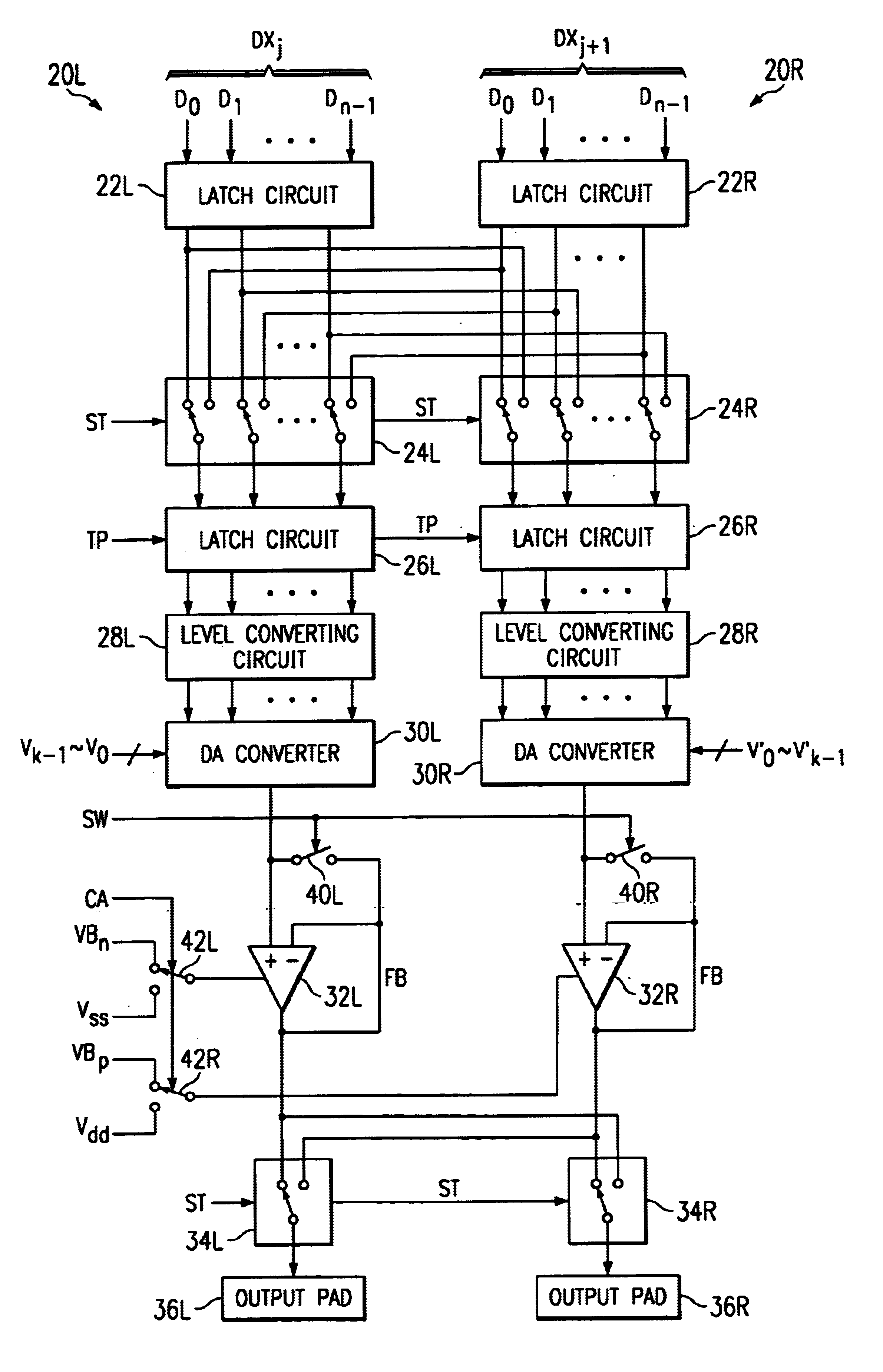
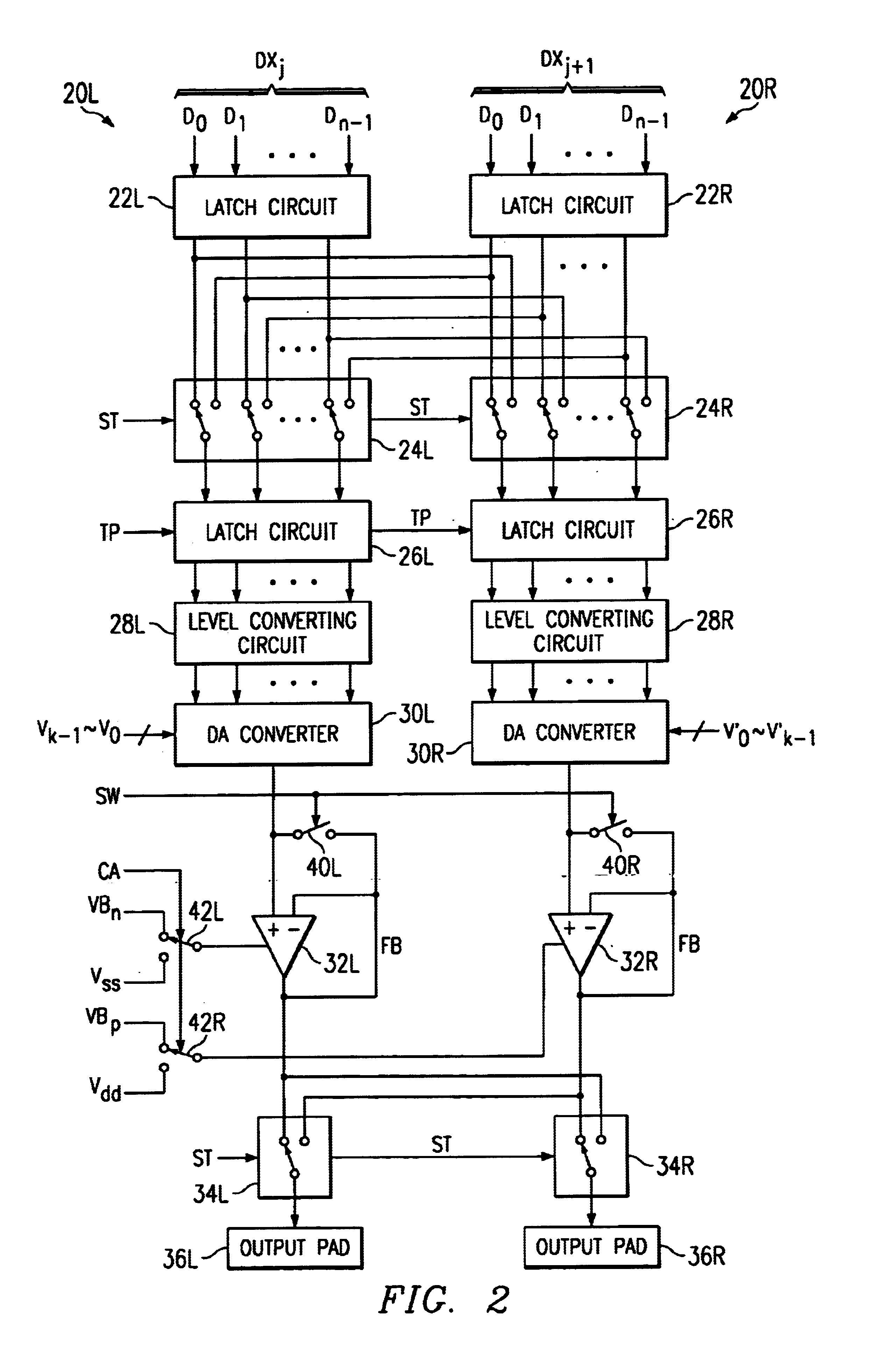
[0032]Preferred embodiments of the present invention will be explained in the following with reference to FIGS. 1-4.

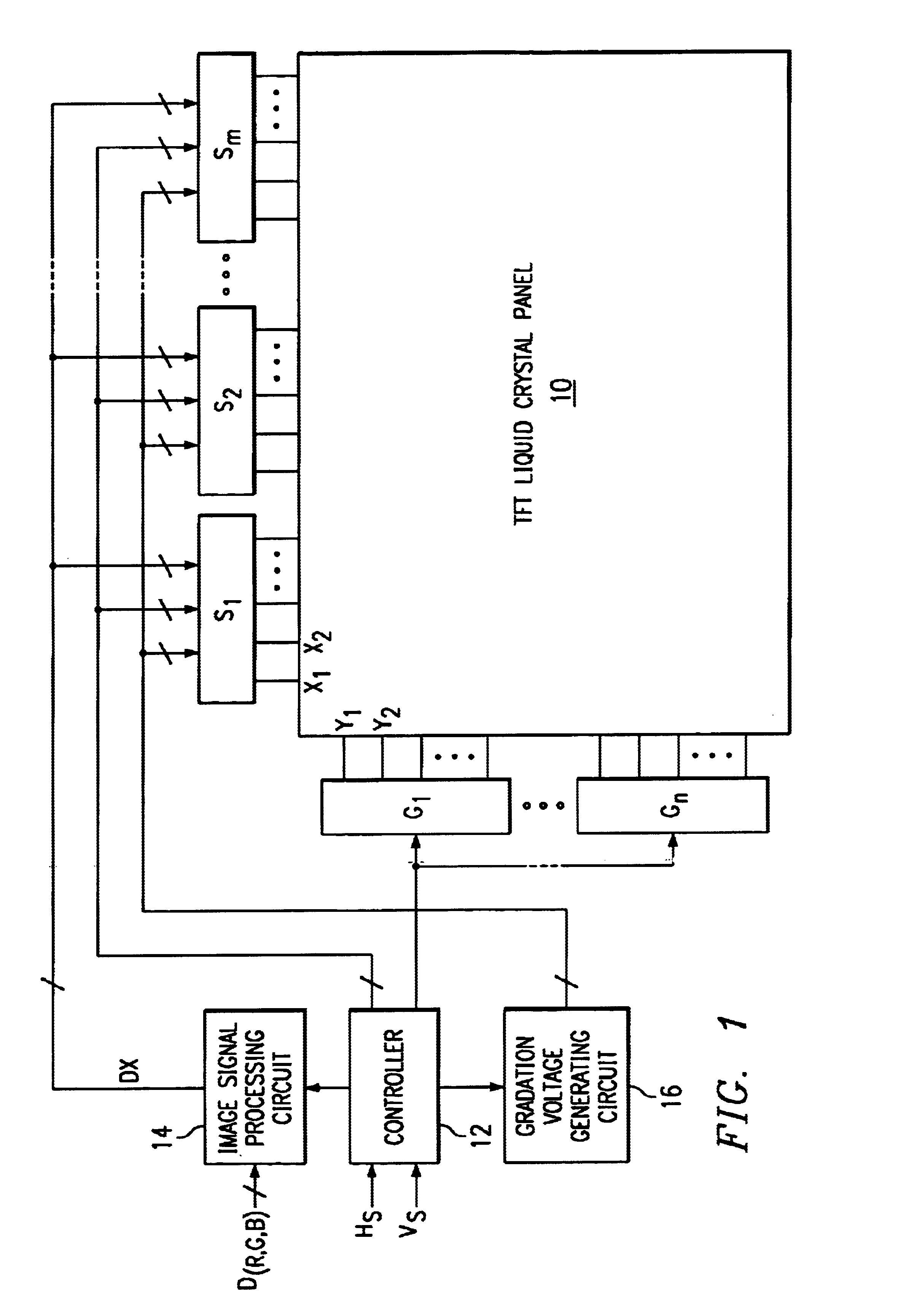
[0033]FIG. 1 is a schematic diagram illustrating the configuration of an active matrix type full-color TFT-LCD using the driving circuit of the present invention.

[0034]The TFT-LCD is comprised of a TFT liquid crystal panel 10 which has the same configuration as that shown in said FIG. 5, gate line drivers G1, G2, . . . which are connected in parallel with each other to drive gate lines Y1, Y2, . . . of said liquid crystal panel 10, signal line (source) drivers S1, S2, . . . which are connected in parallel with each other to drive signal lines X1, X2, . . . of liquid crystal panel 10, controller 12 which controls the operation of each part, image signal processing circuit 14 which performs prescribed signal processing with respect to the image signals to be displayed, and a gradation voltage generating circuit 16 which can generate multiple voltage levels for realizing ...


PUM

PropertyMeasurementUnit
voltageaaaaaaaaaa
voltageaaaaaaaaaa
voltageaaaaaaaaaa

Abstract

The objective of this invention is to compensate or avoid the influence of offset in an easy and efficient manner, to correctly match the voltage of the output signal with the voltage of the input signal, that is, the target value, and to significantly reduce the current consumption. When voltage follower 32L supplies bias voltage VBn to each of constant current source circuits 58L, 60L, it acts as a source-type voltage follower. However, when the bias voltage applied to each of constant current source circuits 58L, 60L is changed from VBn to Vss of the power supply voltage level, each of constant current source circuits 58L, 60L is turned off, and no current flows through them. When the constant current source circuit 58 is turned off in differential input part 44L, the potential at the output terminal (node) NL rises almost to the level of the power supply voltage Vdd. In this way, the driving transistor 62L is also turned off in output part 46L.

Description

FIELD OF THE INVENTION[0001]The present invention pertains to a driving circuit that drives the voltage of an electric load. In particular, the present invention pertains to a voltage follower type driving circuit.BACKGROUND OF THE INVENTION[0002]The signal line driving circuit of a thin film transistor type liquid crystal display (TFT-LCD) that performs multi-gradation display is an application example of this type of driving circuit.[0003]FIG. 5 shows the basic circuit configuration (in part) of a TFT liquid crystal panel. In this type of liquid crystal panel, multiple gate lines Yi−1, Yi, Yi+1 . . . and multiple signal lines Xj−1, Xj, and Xj+1 . . . are arranged in a matrix pattern. A pixel electrode P made of a transparent electroconductive film and a thin film transistor TFT is arranged for the pixel at each cross point. A signal storage capacitance CL for one pixel is formed by the liquid crystal Q sandwiched between each pixel electrode P and counter electrode COM.[0004]All o...

Claims


Application Information

Patent Timeline
Patent Type & Authority Patents(United States)
IPC IPC(8): G09G3/36G11C19/00G02F1/133G09G3/20H03F1/02H03F3/34H03F3/72
CPCG09G3/3688G11C19/00G09G3/3614G09G2310/027G09G2310/0291G09G2310/0294G09G2310/0297G09G2320/02G09G2330/021
Inventor FUKUDA, YASUHIRO
Owner TEXAS INSTR INC
Why Eureka
Try Eureka