Light emitting display, display panel, and driving method thereof

a technology of light-emitting display and display panel, which is applied in the direction of electroluminescent light sources, static indicating devices, instruments, etc., can solve the problems of difficult to obtain high gray, difficult to represent high gray, and difficult control of pixel circuit by fine current isub>data, etc., and achieves the effect of requiring a lot of time for charging the data lin

Active Publication Date: 2005-07-19
SAMSUNG DISPLAY CO LTD
View PDF9 Cites 279 Cited by
  • Summary
  • Abstract
  • Description
  • Claims
  • Application Information

AI Technical Summary

Benefits of technology

[0020]In one aspect of the present invention, a light emitting display is provided that includes a display panel on which a plurality of data lines for transmitting the data current that displays video signals, a plurality of scan lines for transmitting a select signal, and a plurality of pixel circuits formed at a plurality of pixels defined by the data lines and the scan lines are formed. The pixel circuit includes: a light emitting element for emitting light corresponding to the applied current; a first transistor, having first and second main electrodes and a control electrode, for supplying a driving current for the light emitting element; a first switch for diode-connecting the first transistor in response to a first control signal; a first storage unit for storing a first voltage corresponding to a threshold voltage of the first transistor in response to a second control signal; a second switch for transmitting a data signal from the data line in response to the select signal from the scan line; a second storage unit for storing a second voltage corresponding to the data current from the first switch; and a third switch for transmitting the driving current from the first transistor to the light emitting element in response to a third control signal. A third voltage determined by coupling of the first and second storage units respectively storing the first and second voltages is applied to the first transistor to supply the driving current to the light emitting element. The second control signal is enabled, the select signal is enabled, and the third control signal is then enabled in order. The pixel circuit further includes a fourth switch turned on in response to the second control signal, and coupled to a control electrode of the first transistor. The second storage unit is formed by a first capacitor coupled between the control electrode and the first main electrode of the first transistor. The first storage unit is formed by parallel coupling of a second capacitor coupled between the first main electrode of the first transistor and a second end of the fourth switch, and the first capacitor. The second control signal is the select signal from the scan line, and the fourth switch responds in the disable interval of the select signal. The first control signal includes a select signal from the previous scan line and a select signal from the current scan line. The first switch includes a second transistor for diode-connecting the first transistor in response to the select signal from the previous scan line, and a third transistor for diode-connecting the first transistor in response to the select signal from the current scan line. The second control signal includes a select signal from the previous scan line, and the third control signal. The pixel circuit further includes a fifth switch coupled in parallel to the fourth switch. The fourth and fifth transistors are respectively turned on in response to the select signal from the previous scan line and the third control signal.
[0021]In another aspect of the present invention, a display panel of a light emitting display, on which a plurality of data lines for transmitting the data current that displays video signals, a plurality of scan lines for transmitting a select signal, and a plurality of pixel circuits formed at a plurality of pixels defined by the data lines and the scan lines are formed. The pixel circuit includes: a first transistor having a first main electrode coupled to a first power supplying a first voltage; a first switch coupled between a second main electrode of the first transistor and the data line, and being controlled by a first select signal from the scan line; a second switch controlled by a first control signal to diode-connect the first transistor; a third switch having a first end coupled to a control electrode of the first transistor, and being controlled by a second control signal; a fourth switch having a first end coupled to a second main electrode of the first transistor, and being controlled by a third control signal; a light emitting element, coupled between a second end of the fourth switch and a second power supplying a second voltage, for emitting light corresponding to the applied current; a first storage unit coupled between the control electrode and the first main electrode of the first transistor when the third switch is turned on; and a second storage unit coup

Problems solved by technology

However, the conventional pixel circuit following the voltage programming method has a problem in that it is difficult to obtain high gray because of deviation of a threshold voltage VTH of a TFT and deviations of electron mobility caused by non-uniformity of an assembly process.
Also, since the value β in Equation 1 changes because of the deviation of the mobility,

Method used


Image

  • Light emitting display, display panel, and driving method thereof
  • Light emitting display, display panel, and driving method thereof
  • Light emitting display, display panel, and driving method thereof

Examples


first embodiment

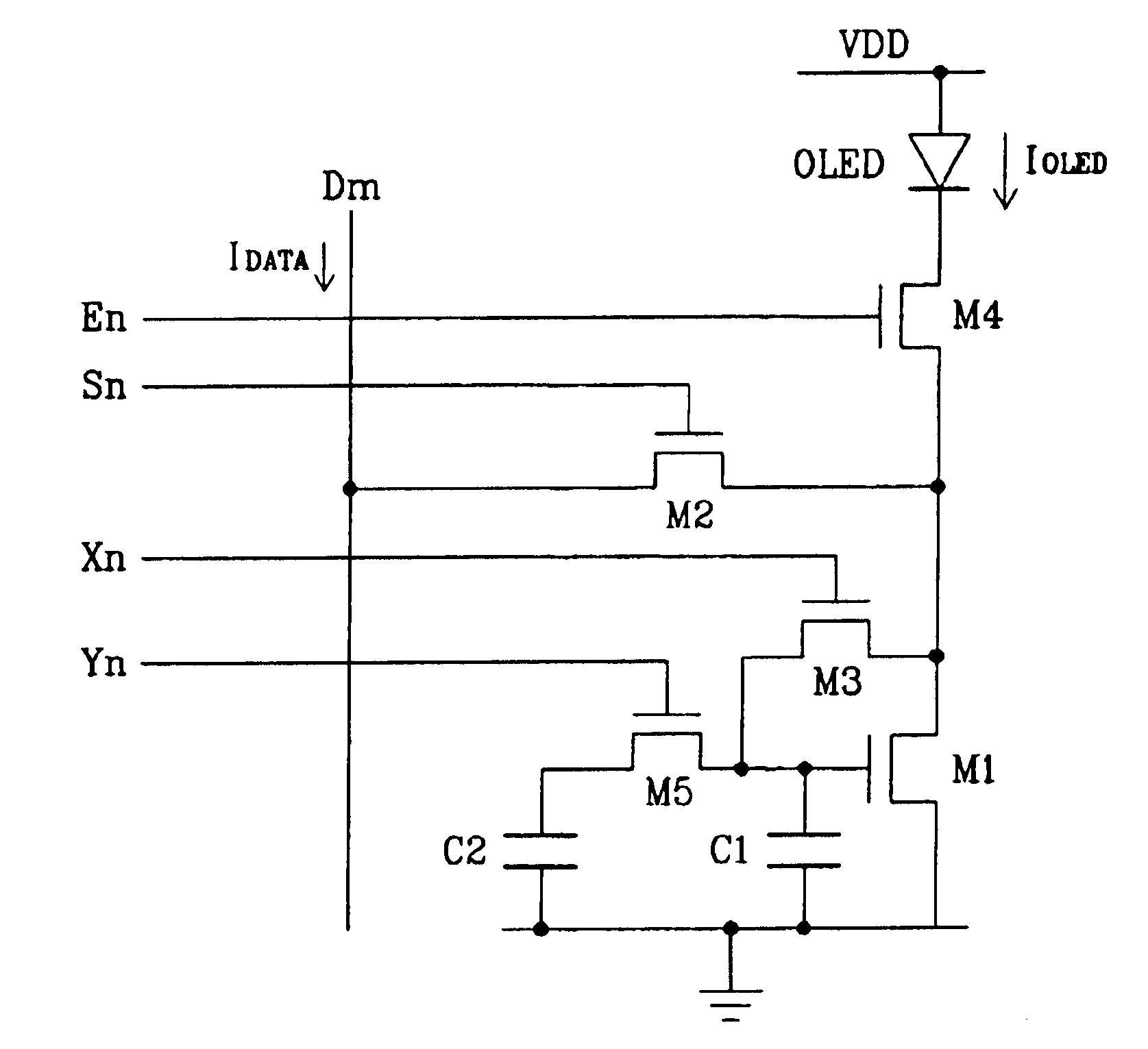
[0041]Referring to FIG. 6, an operation of the pixel circuit according to the present invention will now be described in detail.

[0042]As shown, in interval T1, transistor M5 is turned on because of low-level control signal CS2n, and capacitors C1 and C2 are coupled in parallel between the gate and the source of transistor M1. Transistor M3 is turned on because of low-level control signal CS1n, transistor M1 is diode-connected, and the threshold voltage VTH of transistor M1 is stored in capacitors C1 and C2 coupled in parallel because of diode-connected transistor M1. Transistor M4 is turned off because of high-level emit signal EMn, and the current to the OLED is intercepted. That is, in interval T1, the threshold voltage VTH of transistor M1 is sampled to capacitors C1 and C2.

[0043]In interval T2, control signal CS2n becomes high level to turn off transistor M5, and select signal SEn becomes low level to turn on transistor M2. Capacitor C2 is floated while charged with voltage, bec...

second embodiment

[0048]FIG. 7 shows an equivalent circuit diagram of the pixel circuit according to the present invention, and FIG. 8 shows a driving waveform diagram for driving the pixel circuit of FIG. 7.

[0049]The pixel circuit of FIG. 7 includes NMOS transistors M1 through M5, and their coupling structure is symmetric with the pixel circuit of FIG. 5. In detail, transistor M1 has a source coupled to the reference voltage, a gate coupled to transistor M5, and transistor M3 is coupled between the gate and a drain of transistor M1. Capacitor C1 is coupled between the reference voltage and the gate of transistor M1, and capacitor C2 is coupled between the reference voltage and a first end of transistor M5. A second end of transistor M5 is coupled to the gate of transistor M1, and control signals CS1n and CS2n from scan lines Xn and Yn are respectively applied to the gates of transistors M3 and M5. Transistor M2 transmits data current IDATA from data line Dm to transistor M1 in response to select sig...

third embodiment

[0054]FIG. 9 shows an equivalent circuit diagram of the pixel circuit according to the present invention, and FIG. 10 shows a driving waveform diagram for driving the pixel circuit of FIG. 9.

[0055]As shown in FIG. 9, the pixel circuit has the same configuration as the first embodiment except for transistors M2 and M5. Transistor M2 includes an NMOS transistor, and gates of transistors M2 and M5 are coupled in common to scan line Sn. That is, transistor M5 is driven by select signal SEn from scan line Sn.

[0056]Referring to FIG. 10, in interval T1, transistors M3 and M5 are turned on because of low-level control signal CS1n and select signal SEn. Transistor M1 is diode-connected because of turned-on transistor M3, and the threshold voltage VTH at transistor M1 is stored in capacitors C1 and C2. Also, transistor M4 is turned off because of high-level emit signal EMn, and the current flow to the OLED is intercepted.

[0057]In interval T2, select signal SEn becomes high level to turn trans...


PUM


Abstract

A light emitting display for compensating for the threshold voltage of transistor or mobility and fully charging a data line. A transistor and first through third switches are formed on a pixel circuit of an organic EL display. The transistor supplies a driving current for emitting an organic EL element (OLED). The first switch diode-connects the transistor. A first storage unit stores a first voltage corresponding to a threshold voltage of the transistor. A second switch transmits a data current in response to a select signal. A second storage unit stores a second voltage corresponding to the data current. A third switch transmits the driving current to the OLED. A third voltage determined by coupling of the first and second storage units is applied to a transistor to supply the driving current to the OLED.

Description

CROSS REFERENCE TO RELATED APPLICATION[0001]This application claims priority to and the benefit of Korea Patent Application No. 2003-20432 filed on Apr. 1, 2003 in the Korean Intellectual Property Office, the content of which is incorporated herein by reference.BACKGROUND OF THE INVENTION[0002](a) Field of the Invention[0003]The present invention relates to a light emitting display, a display panel, and a driving method thereof. More specifically, the present invention relates to an organic electroluminescent (EL) display.[0004](b) Description of the Related Art[0005]In general, an organic EL display electrically excites a phosphorous organic compound to emit light, and it voltage- or current-drives N×M organic emitting cells to display images. As shown in FIG. 1, the organic emitting cell includes an anode of indium tin oxide (ITO), an organic thin film, and a cathode layer of metal. The organic thin film has a multi-layer structure including an emitting layer (EML), an electron tr...

Claims


Application Information

Patent Timeline
IPC IPC(8): G09G3/36G09G3/14G09G3/04G09G3/32G09G3/30G09G3/20H05B33/14H05B33/00H01L51/50G11C11/00
CPCG09G3/325G09G2300/0852G09G2300/0861G09G2310/0251G09G2310/0262G09G2320/0223G09G2320/0233G09G3/30
Inventor KWON, OH-KYONG
Owner SAMSUNG DISPLAY CO LTD
Why Eureka
Try Eureka