
Constant delay zero standby differential logic receiver and method
a technology of differential logic and constant delay, applied in the field ofdifferential, can solve problems such as data clocked in early or late, data that is clocked in early, and may not be accurate, and achieve the effect of timing error (unexpected delay) in single-ended drivers
- Summary
- Abstract
- Description
- Claims
- Application Information
AI Technical Summary
Benefits of technology
Problems solved by technology
Method used
Image

Examples
Embodiment Construction
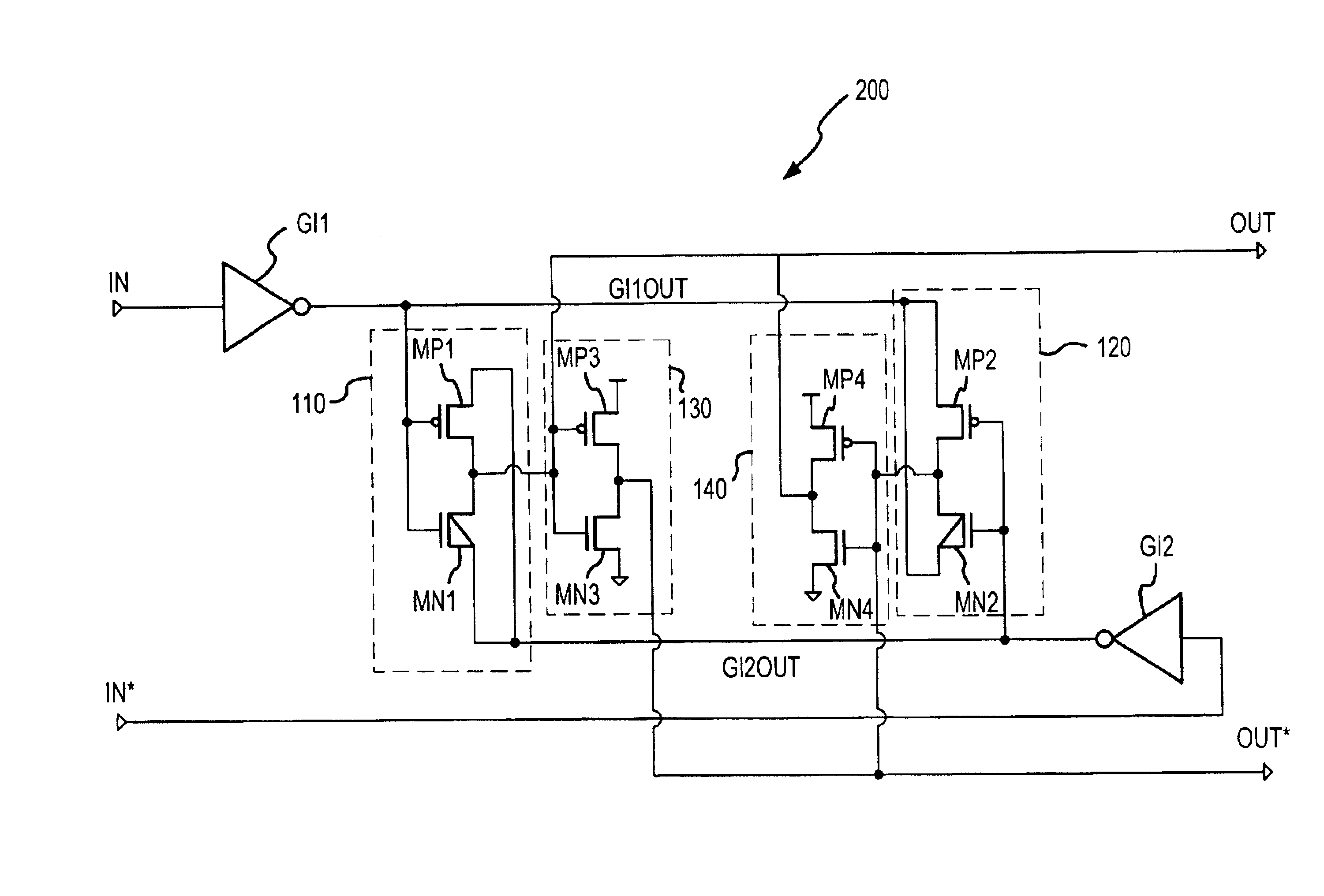
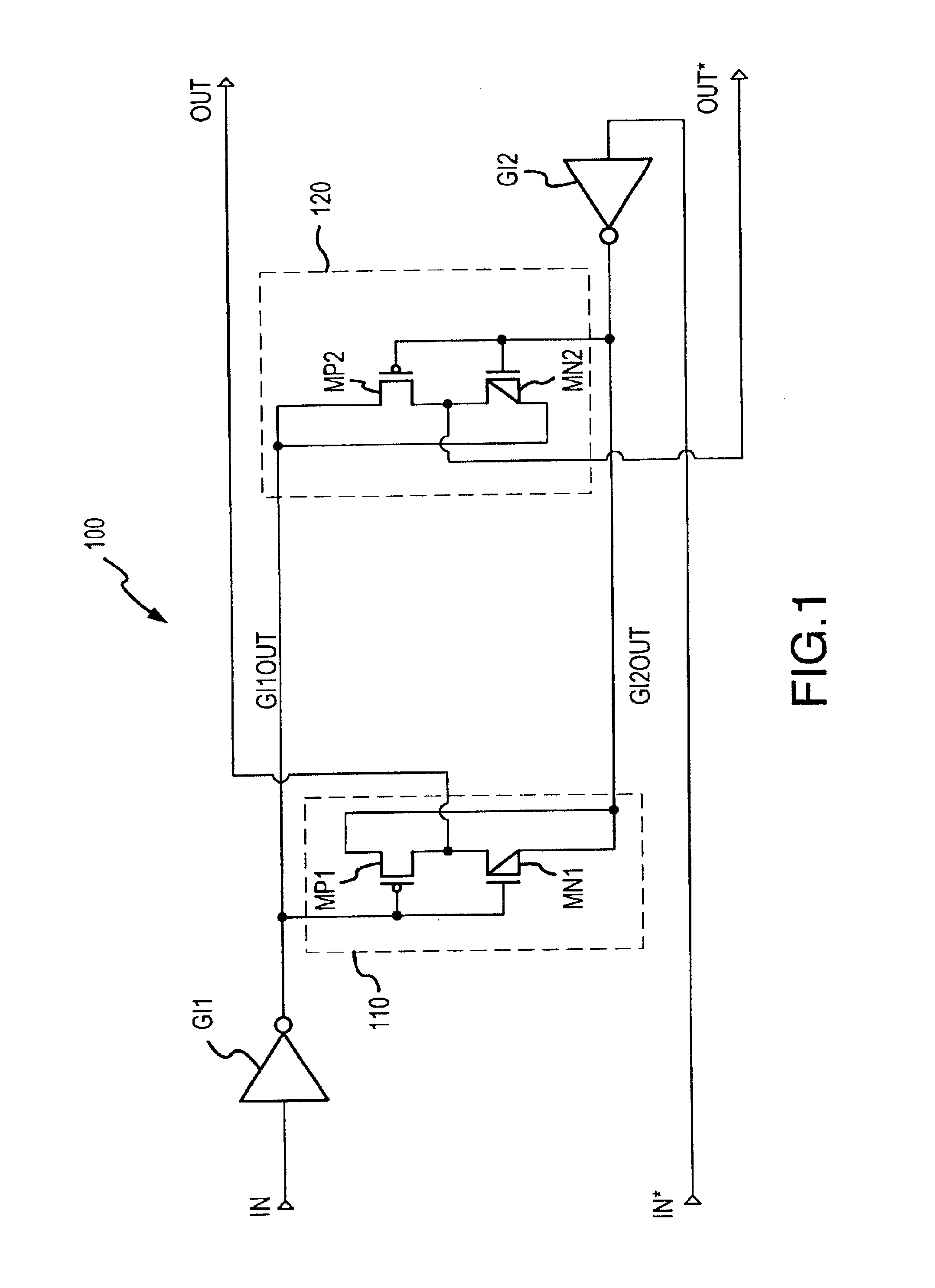
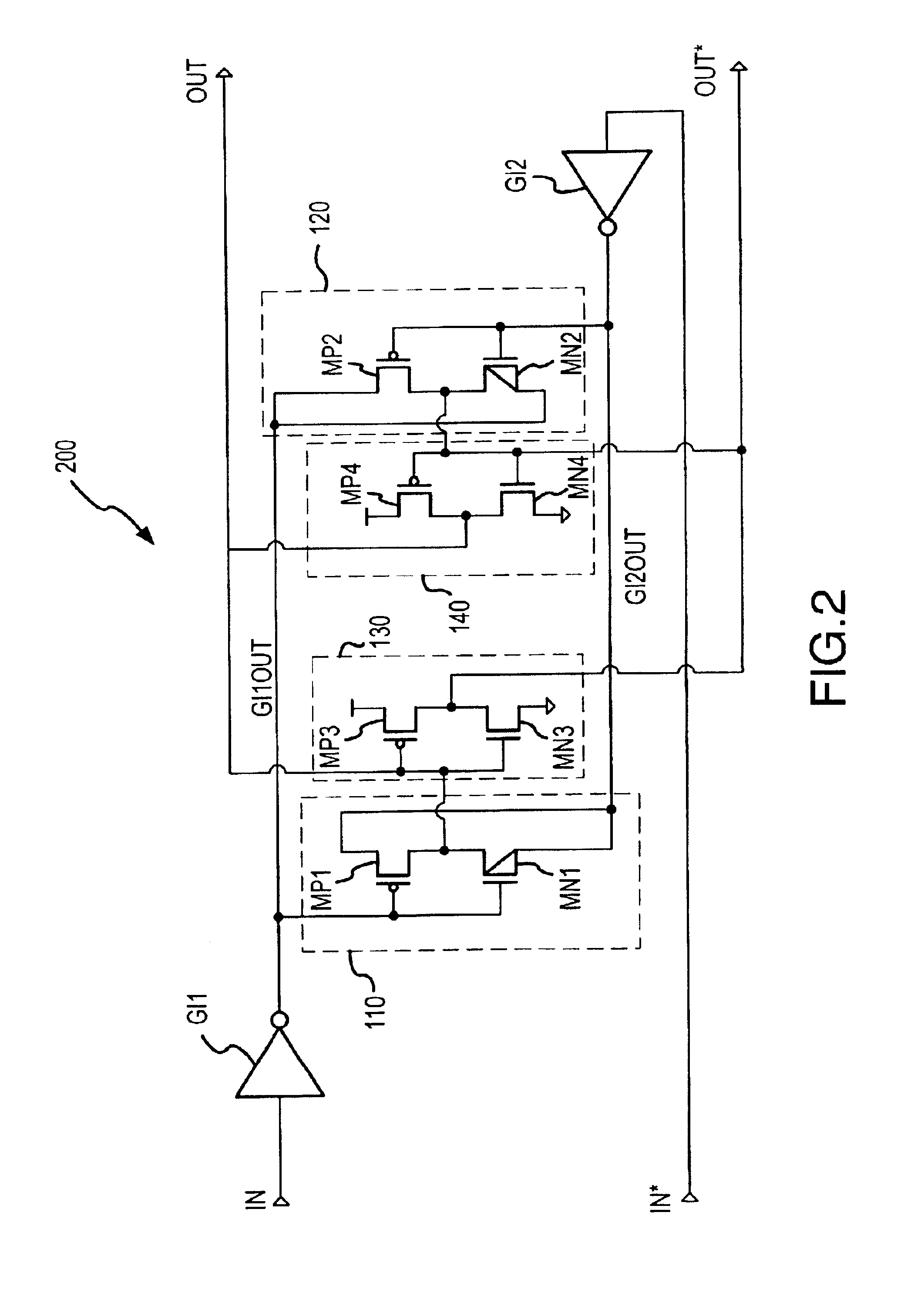
[0025]A common mode receiver 100 according to one example of the present invention is depicted in FIG. 1. The receiver 100 includes a first inverter GI1 coupled to a true input signal IN to produce an inverted signal GI1OUT, and also includes a second inverter GI2 coupled to a complimentary input signal IN* to produce a complimentary signal GI2OUT. The receiver 100 also includes a first pass circuit 110 to provide a true output signal OUT. When differential output signals are desired, as with intermediate drivers, the receiver 100 also includes a second pass circuit 120 to provide a complimentary output signal OUT*.
[0026]The first pass circuit 110 includes a p channel transistor MP1 and an n channel transistor MN1. Gates of both the transistors MP1 and MN1 are coupled to the output of the first inverter GI1 so that the signal GI1OUT is applied to the gates of the transistors MP1 and MN1. The signal GI1OUT controls the conductive state of the transistors MP1, MN1 and thus constitutes...
PUM
 Abstract
Description
Claims
Application Information