Constant delay zero standby differential logic receiver and method

a differential logic and constant delay technology, applied in pulse manipulation, pulse technique, baseband system details, etc., can solve the problems of data that is clocked in early or late, data that is clocked in early, and may not be accurate,

Active Publication Date: 2006-01-19
MICRON TECH INC
View PDF28 Cites 1 Cited by
  • Summary
  • Abstract
  • Description
  • Claims
  • Application Information

AI Technical Summary

Benefits of technology

[0009] An integrated circuit in accordance with the invention includes a differential receiver circuit that consumes substantially no standby power, has constant propagation delay regardless of the input common mode bias, has acceptable common mode rejection and includes first and second pass circuits and buffers to receive differential input signals. The first pass circuit provides a “true” output signal when there is a difference between a “true” buffered signal and a “complimentary” buffered signal. The second pass circuit provides a “complementary” output signal when there is a difference between the “complimentary” buffered signal and the “true” buffered signal. The differential receiver circuit further includes cross coupled inverters latching the true and complimentary output signals in complementary states, and final drive buffers for amplifying the true and complimentary output signals.

Problems solved by technology

One challenge in such circuits is to distribute signals, such as clock and data strobe signals, over distances that are characterized as long distances, at least long as compared to the time periods available for rise times, fall times, pulse widths, etc.
Increases or decreases in duty cycle of the strobe, for any reason, will result in data clocked in early or late.
At high frequencies, data that is clocked in early, may not be accurate since the voltages on the data lines many not have had time to settle to a level that is representative of the data value.
Intermediate drivers tend to introduce duty cycle skew as well.
Common mode bias that couples into the differential signal from stray signals or from supply noise can cause timing error (undesired delays) in single ended drivers.
However, a problem remains with the use of known differential receivers.
Thus, differential receivers consume a significant current whether or not differential signals are actually needed to be processed through the receiver at the particular time.
In many applications it would be impractical to use as many differential pair receivers in critical clock paths as might otherwise be desired since a high standby current would be consumed.
Another problem is that this type of differential receiver has a different propagation delay depending on the voltage of the cross point of the differential input signals (as when a common mode voltage bias is coupled into the differential input signals).
A varying propagation delay is unacceptable for critical timing paths, especially at high frequencies.

Method used


Image

  • Constant delay zero standby differential logic receiver and method
  • Constant delay zero standby differential logic receiver and method
  • Constant delay zero standby differential logic receiver and method

Examples


Embodiment Construction

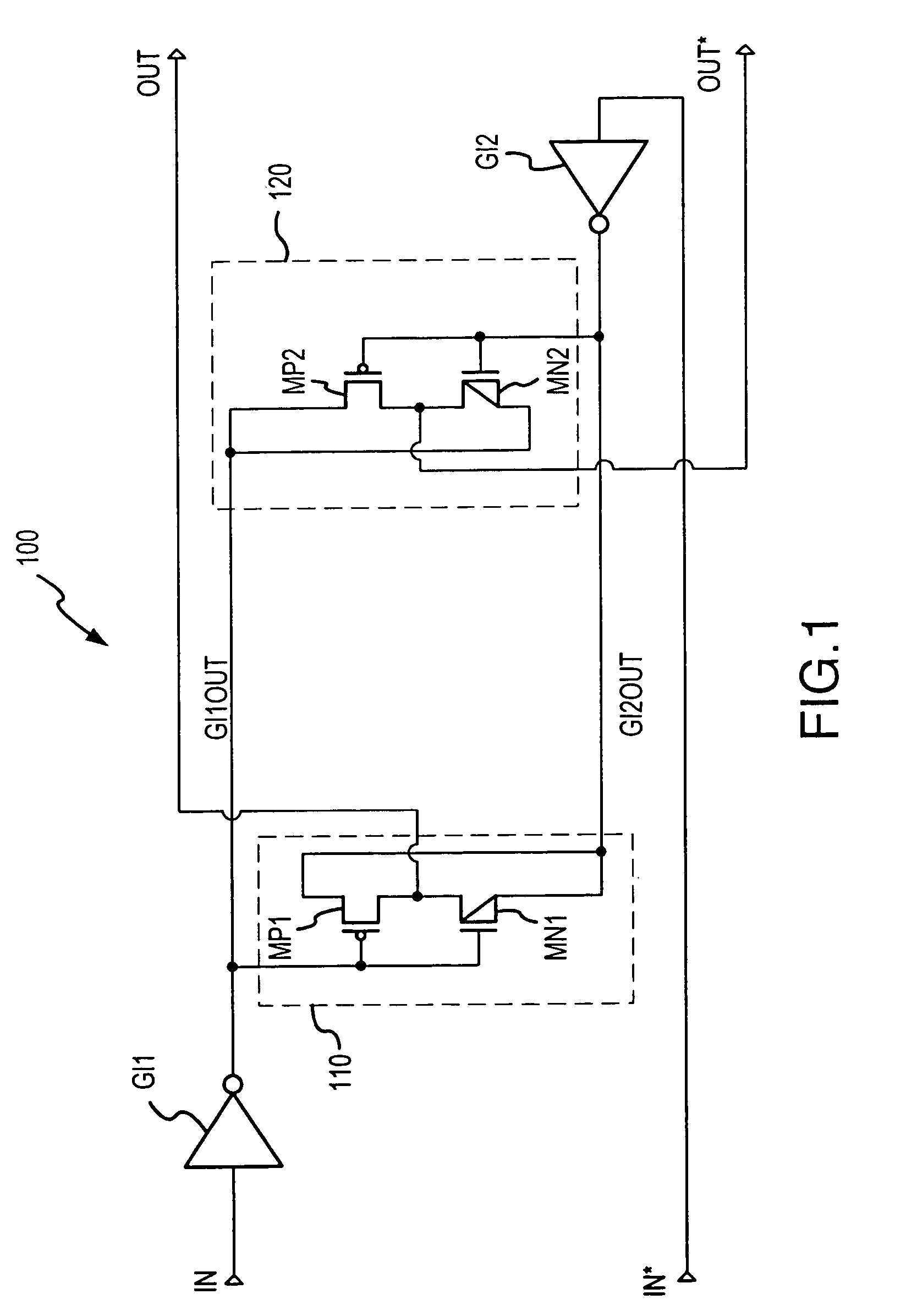
[0025] A common mode receiver 100 according to one example of the present invention is depicted in FIG. 1. The receiver 100 includes a first inverter GI1 coupled to a true input signal IN to produce an inverted signal GI1OUT, and also includes a second inverter GI2 coupled to a complimentary input signal IN* to produce a complimentary signal GI2OUT. The receiver 100 also includes a first pass circuit 110 to provide a true output signal OUT. When differential output signals are desired, as with intermediate drivers, the receiver 100 also includes a second pass circuit 120 to provide a complimentary output signal OUT*.

[0026] The first pass circuit 110 includes a p channel transistor MP1 and an n channel transistor MN1. Gates of both the transistors MP1 and MN1 are coupled to the output of the first inverter GI1 so that the signal GI1OUT is applied to the gates of the transistors MP1 and MN1. The signal GI1OUT controls the conductive state of the transistors MP1, MN1 and thus constitu...


PUM


Abstract

A differential receiver circuit on an integrated circuit consumes substantially no standby power, has constant propagation delay regardless of the input common mode bias, has acceptable common mode rejection and includes first and second pass circuits and buffers to receive differential input signals. The first pass circuit provides a true output signal based on a differential between the “true” buffered signal and the complimentary buffered signal. The second pass circuit provides a “complementary” output signal based on a differential between the complimentary buffered signal and the “true” buffered signal. The differential receiver circuit rejects common mode biases that may be present on the received differential signals without varying propagation delay times.

Description

TECHNICAL FIELD [0001] The present invention relates to distribution of clock and strobe signals in semiconductor integrated circuits. In particular, the invention relates to differential receivers to receive differential clock and strobe signals. BACKGROUND OF THE INVENTION [0002] Semiconductor integrated circuits, such as memory chips, are becoming physically larger in area, and their operational speeds are becoming faster. One challenge in such circuits is to distribute signals, such as clock and data strobe signals, over distances that are characterized as long distances, at least long as compared to the time periods available for rise times, fall times, pulse widths, etc. With such circuits, it is becoming increasingly more important to maintain correct duty cycle on certain critical signals, such as clock and strobe signals, especially at high frequencies. However, when a single pulse is propagated through many driver receiver pairs, the duty cycle (e.g., as measured by the po...

Claims


Application Information

Patent Timeline
Patent Type & Authority Applications(United States)
IPC IPC(8): H03K9/00H03K5/003H03K5/156H03K19/003H04L25/02H04L25/10
CPCH03K5/003H03K5/1565H04L25/10H04L25/0274H04L25/0292H03K19/00323H01K9/00H03D3/22H04L27/06H04L27/14
Inventor PENNEY, DANIEL B.
Owner MICRON TECH INC
Why Eureka
Try Eureka