Low forward voltage drop schottky barrier diode and manufacturing method therefor

a technology of schottky barrier diodes and manufacturing methods, which is applied in the direction of diodes, semiconductor devices, electrical apparatus, etc., can solve the problems of increasing the cost of chips, increasing the leakage current of devices, and reducing the reverse blocking voltage of devices, so as to achieve the effect of low forward voltage drop

Inactive Publication Date: 2005-07-26
ONIZUKA ELECTRONICS
View PDF2 Cites 18 Cited by
  • Summary
  • Abstract
  • Description
  • Claims
  • Application Information

AI Technical Summary

Benefits of technology

[0009]It is an object of the present invention to provide a Schottky barrier diode which can provide a low forward voltage drop and manufacturing method therefor.
[0010]It is another object of the present invention to provide a low forward voltage drop Schottky barrier diode which can achieve a super low forward voltage without changing the metal and the metallization mechanism and also can achieve a better trade-off between the forward voltage drop and the breakdown voltage through an optimized association of the size of the puckered structure and the depth of the unit trench.
[0012]It is an additional object of the present invention to provide an integrated structure of a SBD and a MOSFET having the characteristics of low impedance, low forward voltage drop, and an improved body-diode reverse recovery for improving the efficiency of the total electric equipment.

Problems solved by technology

However, this method also increases the cost of the chip.
The other method is to use a barrier metal with a low barrier height, but it will increase the leakage current of the device.
It also reduces the reverse blocking voltage of the device and degrades the performance of the device at high temperature.
Moreover, the development of a new barrier metallization process is a time consuming procedure due to the sophisticated chemistry and metallurgy at the metal and silicon interface.
Furthermore, from the manufacturer's viewpoint, it would be a risk to change the barrier metal because some negative effect might be introduced to the manufacturing control and the product yield, as well as contamination control in the fabrication.
However, these conventional schemes only provide a limited forward voltage drop reduction due to the limitation of silicon surface area.

Method used


Image

  • Low forward voltage drop schottky barrier diode and manufacturing method therefor
  • Low forward voltage drop schottky barrier diode and manufacturing method therefor
  • Low forward voltage drop schottky barrier diode and manufacturing method therefor

Examples


Embodiment Construction

[0039]The present invention will now be described more specifically with reference to the following embodiments. It is to be noted that the following descriptions of preferred embodiments of this invention are presented herein for purpose of illustration and description only; it is not intended to be exhaustive or to be limited to the precise form disclosed.

[0040]The present invention is related to the structure of the SBD (Schottky Barrier Diode) and the manufacturing method therefor to achieve a super low forward voltage without changing the metal and the metallization mechanism of SBD.

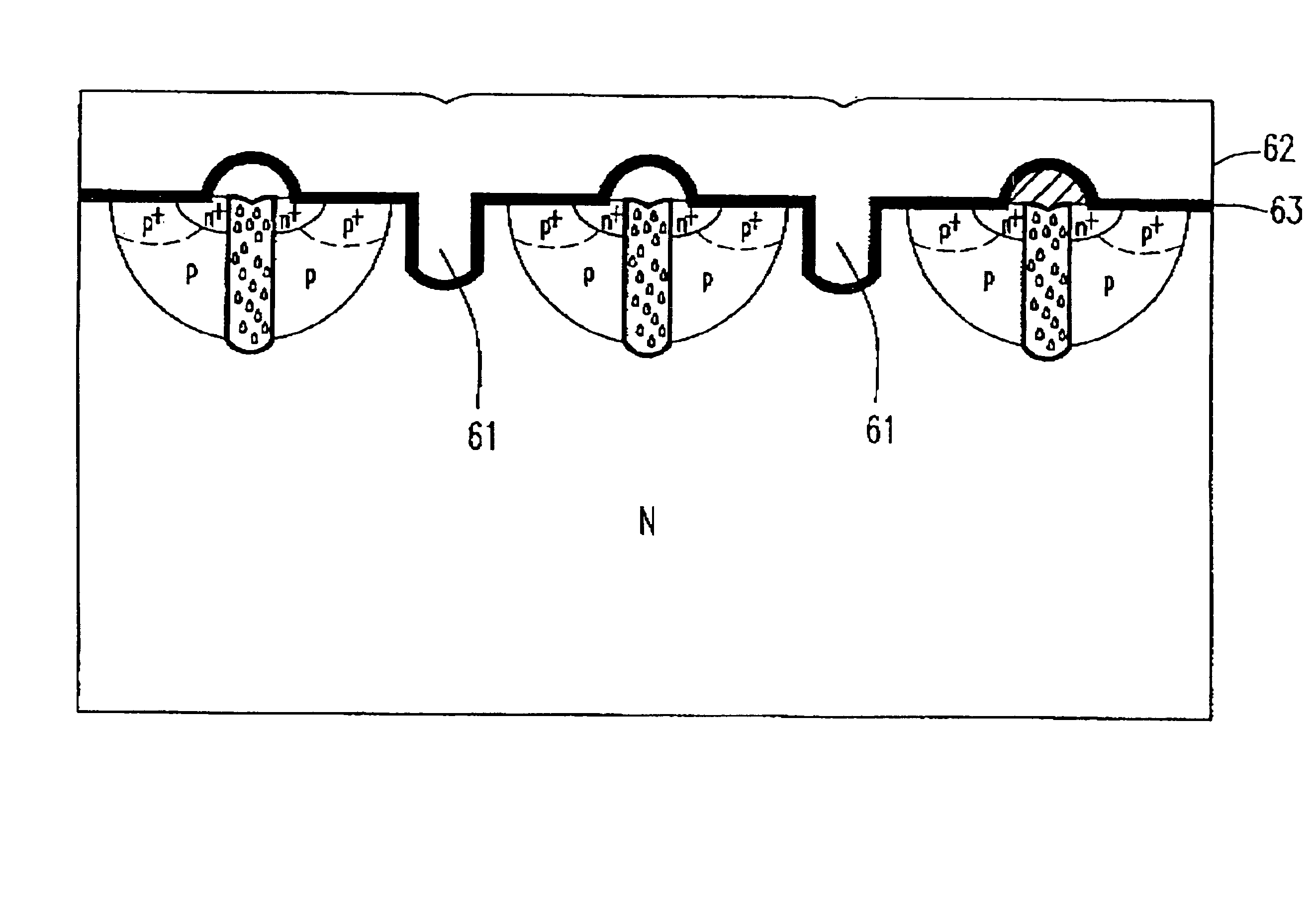
[0041]Please refer to FIG. 6 illustrating a SBD schematic structure view of a preferred embodiment according to the present invention. As shown in FIG. 6, it shows the manufacturing method of the SBD. Firstly, a silicon chip 60 is etched to form plural trenches 61, wherein the silicon chip 60 could be to be silicon or silicon carbon, so that the surface of the silicon chip 60 will become a “puckered...


PUM

PropertyMeasurementUnit
depthaaaaaaaaaa
breakdown voltageaaaaaaaaaa
trench depthaaaaaaaaaa

Abstract

A new low forward voltage drop Schottky barrier diode and its manufacturing method are provided. The method includes steps of providing a substrate, forming plural trenches on the substrate, and forming a metal layer on the substrate having plural trenches thereon to form a barrier metal layer between the substrate and the surface metal layer for forming the Schottky barrier diode.

Description

RELATED APPLICATIONS[0001]This application claims priority to Taiwan Application Serial No. 091103067, filed Feb. 21, 2002.BACKGROUND[0002]1. Field of the Invention[0003]This invention relates to a Schottky barrier diode and a manufacturing method therefor, and more particular to a low forward voltage drop Schottky barrier diode and a manufacturing method therefor.[0004]2. Background of the Invention[0005]Recently, Schottky barrier diodes have been extensively used in a DC—DC converter, a VRM (voltage regulator module), a telecom / server, an adaptor, and a charger. Please refer to FIG. 1 which shows a schematic structure view of a conventional Schottky barrier diode. As shown in FIG. 1, the manufacturing method of the Schottky barrier diode (SBD) includes forming a barrier metal layer 12 followed by depositing a metal layer 11 on a silicon chip 10. The simulation result of a current distribution in the forward conduction mode in the conventional SBD is shown in FIG. 2.[0006]Among all...

Claims


Application Information

Patent Timeline
Patent Type & Authority Patents(United States)
IPC IPC(8): H01L29/78H01L21/02H01L21/329H01L29/66H01L27/06H01L29/872
CPCH01L27/0629H01L29/417H01L29/41766H01L29/66143H01L29/7806H01L29/7813H01L29/872
Inventor ZENG, JUNZHOU, MING-JIANGWU, TZONG-SHIANN
Owner ONIZUKA ELECTRONICS
Why Eureka
Try Eureka