Method for electrodeposited film formation, method for electrode formation, and apparatus for electrodeposited film formation

a technology of electrodeposited film and electrode, applied in the direction of electrolysis components, liquid/solution decomposition chemical coatings, coatings, etc., can solve the problems of thermal diffusion giving rise to overhangs on the edges of plating, non-electrolytic plating,

Inactive Publication Date: 2005-08-02
FUJIFILM BUSINESS INNOVATION CORP
View PDF4 Cites 8 Cited by
  • Summary
  • Abstract
  • Description
  • Claims
  • Application Information

AI Technical Summary

Benefits of technology

[0016]To solve the above-noted problems, according to one aspect of this invention, there is provided a method for electrodeposited film formation by which a surface of an object to be treated, the surface at least permitting generation of charged particles when irradiated with a laser beam, is irradiated with a pulse laser whose pulse width is less than a picosecond; almost solely electrons are excited on the surface of the object to be treated to generate a state of non-equilibrium in either temperature or energy between the electrons and a grid; and an electrodeposited film is formed on the surface of the object to be treated using the electrons excited in that state of non-equilibrium.
[0017]According to another aspect of the invention, there is provided a method for electrodeposited film formation by which a surface of an object to be treated, the surface at least permitting generation of charged particles when irradiated with a laser beam, is irradiated with a pulse l...

Problems solved by technology

Non-application of a bias voltage would result in non-electrolytic plating.
There is another problem in the conventional application to plating that, since it is a thermal process, thermal diffusion gives rise to overhangs on the edges of plating as illustrated in FIG.
Furthermore, for electrode formation, in man...

Method used


Image

  • Method for electrodeposited film formation, method for electrode formation, and apparatus for electrodeposited film formation
  • Method for electrodeposited film formation, method for electrode formation, and apparatus for electrodeposited film formation
  • Method for electrodeposited film formation, method for electrode formation, and apparatus for electrodeposited film formation

Examples


embodiment 1

(Embodiment 1)

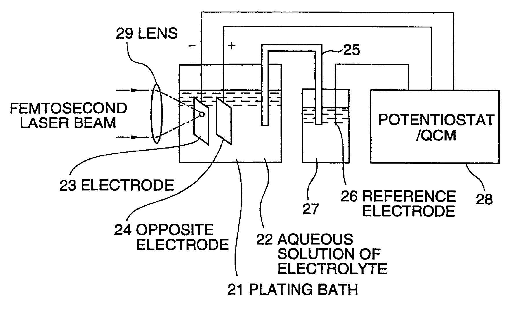
[0066]FIG. 4 and FIG. 5 show variations in electric charge generated by the fs laser, the cw laser and the ns laser relative to the laser beam intensity. FIG. 4 illustrates a case in which an aqueous solution of Pt (H2PtCl6; 1 g / (CH3COO)2Pb; 10 mg / water 30cc) was used, and FIG. 5, a case in which an aqueous solution of Zn (ZnCl2; 20 g / water 80cc) was used, both as the electrolyte solution 22.

[0067]The bias voltage between the electrode 23 and the opposite electrode 24 was −300 mV for the aqueous solution of Pt and −1.1 V for the aqueous solution of Zn. The electrode 23 was one of Au, and the opposite electrode 24, one of platinum black.

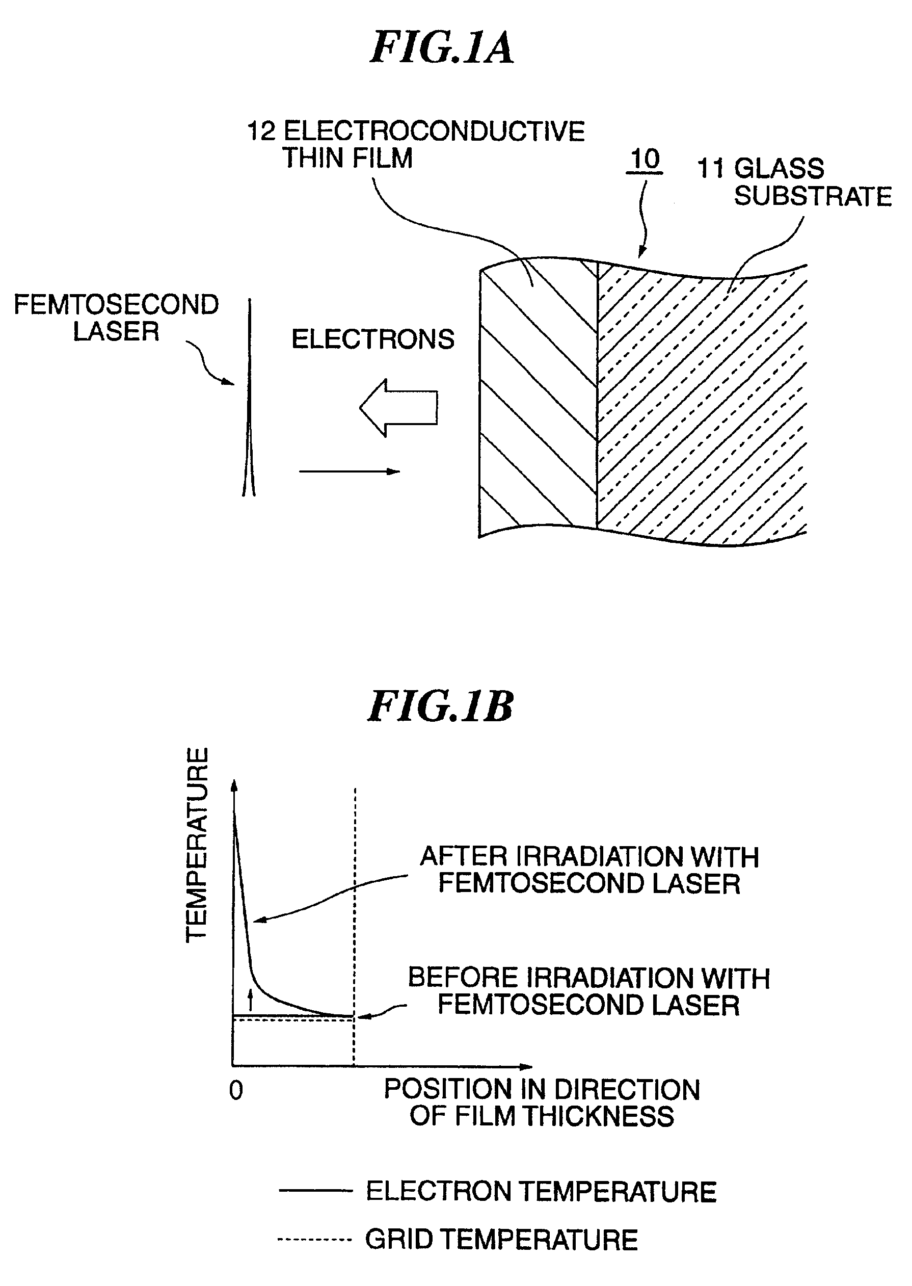
[0068]It is seen from these FIG. 4 and FIG. 5 that, whichever the electrolyte solution was, the electric charge generated under irradiation with the fs laser was four to ten times as much as that generated under irradiation with the cw laser or the ns laser. This reveals that electrons were more efficiently taken out when under irradiati...

embodiment 2

(Embodiment 2)

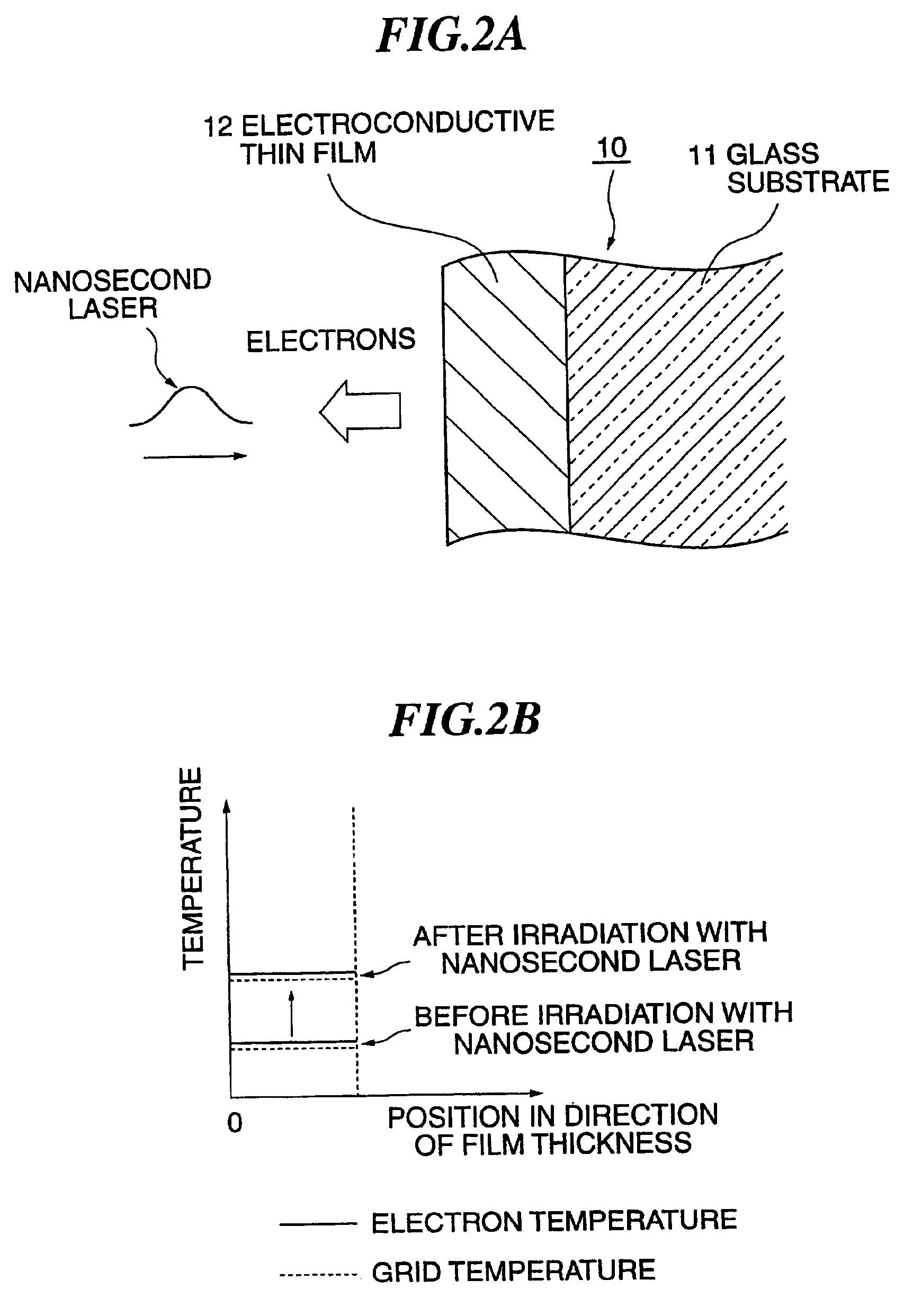
[0069]FIG. 6 shows variations in electrode weight when under irradiation with the fs laser (fs pulse in FIG. 6) and under irradiation with the ns laser (ns pulse in FIG. 6) In this case the irradiation intensity of the fs laser was 2.8 W / cm2, and that of the ns laser was 12.7 W / cm2. The electrolyte solution used in this case was H2PtCl6; 1 g / (CH3COO)2Pb; 10 mg / water 30 cc; the bias voltage was −300 mV, the electrode 23 was one of Au, and the opposite electrode 24 was one of platinum black. Variations in resonance frequency Δf in the negative direction matched increases in weight.

[0070]It is seen from this FIG. 6 that, while the electrode weight increased, i.e. plating was formed, when under irradiation with the fs laser, no plating was formed when under irradiation with the ns laser in spite of its more than four times as great luminous intensity than that of the fs laser. By direct visual observation, too, spotty formation of plating was witnessed when under irradiati...

embodiment 3

(Embodiment 3)

[0072]In addition to the foregoing, the following study was carried out to finally confirm that the phenomenon resulting from irradiation with the femtosecond laser in this mode of implementing the invention derives from hot electrons.

[0073]In plating formation by a thermo-electromotive force, the laser beam is absorbed by the substrate and generates an electromotive force. For this reason, as illustrated in FIG. 7, where the substrate 31 is made of a transparent material such as glass, plating is similarly formed irrespective of whether the laser beam comes incident on the front side of the thin-film electrode 32 formed by vapor deposition or otherwise as indicated by the arrow FL in the figure (hereinafter referred to as front side incidence) or it comes incident on the backside through the transparent substrate 31 as indicated by the arrow BK (hereinafter called the backside incidence). As a matter of fact, Reference 2 cited above gives a conclusion attributing the ...


PUM

PropertyMeasurementUnit
Percent by massaaaaaaaaaa
Weightaaaaaaaaaa
Electric potential / voltageaaaaaaaaaa

Abstract

A method permitting less energy consumption and efficient formation of high quality electrodes is provided. An electrode is formed as an electrodeposited film by irradiating the surface of an object to be treated, the surface at least permitting generation of charged particles when irradiated with a laser beam, with a fentosecond laser beam and metal-plating the surface of a substrate using hot electrons generated by this laser irradiation.

Description

[0001]This is a Division of application Ser. No. 09 / 571,864 filed May 16, 2000, which issued as U.S. Pat. No. 6,365,027 on Apr. 2, 2002. The entire disclosure of the prior application is hereby incorporated by reference herein in its entirety.BACKGROUND OF THE INVENTION[0002]1. Field of the Invention[0003]This invention relates to methods for forming an electrodeposited film or an electrode over the surface of an object to be treated using an ultra-short pulse laser.[0004]2. Description of the Related Art[0005]Attempted applications of laser to electrode formation technology can be broadly classified into plating and etching.[0006]The basic principle of application to plating is that an object to be plated soaked in a plating solution is irradiated with a laser beam and the resultant thermo-electromotive force causes part of the object to be plated (see, for instance, Reference 1: specification of the U.S. Pat. No. 4,349,583, and Reference 2: IBMJ. Res. Develop., Vol. 42, No.5, Sept...

Claims


Application Information

Patent Timeline
IPC IPC(8): C25D5/02H01L21/288H01L21/02C23C18/18C25D5/18C25D5/54C25D7/00
CPCC25D5/024H01L21/2885C25D7/00C25D5/006C25D5/011
Inventor TATSUURA, SATOSHISATO, YASUHIROTIAN, MINQUANPU, LYONG SUN
Owner FUJIFILM BUSINESS INNOVATION CORP
Why Eureka
Try Eureka