Apparatus and method for conformal mask manufacturing

a technology of conformal masks and masks, applied in the field of semiconductor manufacturing, can solve the problems of high cost, high manufacturing cost, and large number of fabrication steps, and achieve the effects of reducing the cost of manufacturing

Active Publication Date: 2008-07-03
NEXGENSEMI HLDG INC
View PDF5 Cites 246 Cited by
  • Summary
  • Abstract
  • Description
  • Claims
  • Application Information

AI Technical Summary

Problems solved by technology

The preparation, exposure, development, clean, care, and stripping of resist can increase the number of fabrication steps tenfold, requiring expensive equipment and facilities to establish stable, qualified, and high yield fabrication.
While advances in a number of lithography techniques (e.g., ultraviolet (UV), enhanced ultraviolet (EUV) emersion, maskless emersion, laser, phase-shift, projection ion, and electron beam lithography (EBL)) can enable high-scale production at these dimensions, they are nearing their theoretical limits with respect to wavelength, overlay accuracy, and / or cost.
Pushed to the limit, the weaknesses of each process present difficult problems, and the resulting patterning defects can result in significant yield loss.

Method used


Image

  • Apparatus and method for conformal mask manufacturing
  • Apparatus and method for conformal mask manufacturing
  • Apparatus and method for conformal mask manufacturing

Examples


Embodiment Construction

[0048]Although certain preferred embodiments and examples are disclosed below, it will be understood by those in the art that the invention extends beyond the specifically disclosed embodiments and / or uses of the invention and obvious modifications and equivalents thereof. Thus, it is intended that the scope of the invention herein disclosed should not be limited by the particular disclosed embodiments described below.

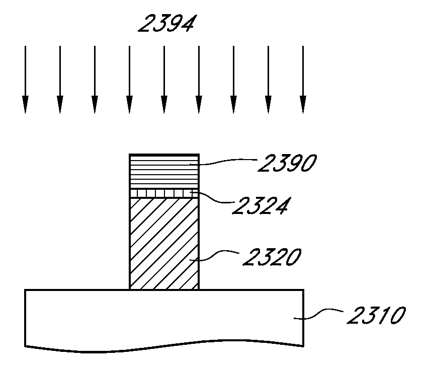
[0049]Smaller device geometries can be achieved by direct writing with a beam of charged particles. Focused ion beam (FIB) systems generally do not have sufficient ion exposure to support high throughput manufacturing. Furthermore, only relatively low speed deflection is available using existing ion optics / deflection electronics methodologies, preventing efficient direct write of layers patterned for semiconductor devices. As such, FIB has been limited to mask (e.g., reticle) and semiconductor repair. As FIB technology progressed, it supported the ability to simultaneo...


PUM

PropertyMeasurementUnit
thickaaaaaaaaaa
thickaaaaaaaaaa
thickaaaaaaaaaa

Abstract

A manufacturing process technology creates a pattern on a first layer using a focused ion beam process. The pattern is transferred to a second layer, which may act as a traditional etch stop layer. The pattern can be formed on the second layer without irradiation by light through a reticle and without wet chemical developing, thereby enabling conformal coverage and very fine critical feature control. Both dark field patterns and light field patterns are disclosed, which may enable reduced or minimal exposure by the focused ion beam.

Description

CROSS-REFERENCE TO RELATED APPLICATIONS[0001]This application claims priority under 35 U.S.C. §119(e) to U.S. Provisional Application Ser. No. 60 / 860,619 filed on Nov. 22, 2006, titled “APPARATUS AND METHOD FOR CONFORMAL MASK MANUFACTURING” (Atty. Docket No. SECL.005PR), which is hereby expressly incorporated by reference in its entirety.BACKGROUND[0002]1. Field[0003]The present application relates to semiconductor manufacturing. More specifically, the present application relates to methods and apparatuses for direct write semiconductor manufacturing.[0004]2. Description of the Related Art[0005]Photolithography has been a key patterning step in most integrated circuit fabrication processes. Resist, a photosensitive organic, is spun on a workpiece, baked, and exposed in a pattern through a reticle, usually by ultraviolet (UV) light. After development and often a second bake, the surface is left partially covered by an inert organic film that resists various treatments to which the wo...

Claims


Application Information

Patent Timeline
Patent Type & Authority Applications(United States)
IPC IPC(8): G03F1/00H01L21/3105H01L21/3065G03C1/00H01L21/306
CPCB82Y10/00B82Y40/00H01J37/3174H01J37/3177H01L21/0331H01L21/0332Y10S430/143H01L21/26533H01L21/28123H01L21/30621H01L29/66659H01L29/7835H01L21/0337
Inventor SCOTT, JEFFREYZANI, MICHAELBENNAHMIAS, MARKMAYSE, MARK
Owner NEXGENSEMI HLDG INC
Why Eureka
Try Eureka