In-plane switching mode active matrix type liquid crystal display device and method of fabricating the same

a liquid crystal display and active matrix technology, applied in the direction of identification means, instruments, optics, etc., can solve the problem of preventing the electrode from being properly driven, and achieve the effect of increasing the aperture ratio

Inactive Publication Date: 2005-08-02
NEC LCD TECH CORP
View PDF17 Cites 99 Cited by
  • Summary
  • Abstract
  • Description
  • Claims
  • Application Information

AI Technical Summary

Benefits of technology

[0026]In view of the above-mentioned problems in the conventional liquid crystal display devices, it is an object of the present invention to provide an in-plane switching (IPS) mode liquid crystal display device which is capable of solving the vertical cross-talk problem and increasing an aperture ratio.
[0027]Specifically in comparison with the above-mentioned conventional liquid crystal display devices, the first object of the present invention is to provide an IPS mode liquid crystal display device which is capable of preventing occurrence of vertical cross-talk without reduction in an aperture ratio.

Problems solved by technology

However, this structure is accompanied with a problem that since a transparent material has a high resistance, there would be generated a voltage difference which would prevent electrodes from being properly driven for displaying images, as pointed out in the above-mentioned Japanese Unexamined Patent Publication No. 9-236820.

Method used


Image

  • In-plane switching mode active matrix type liquid crystal display device and method of fabricating the same
  • In-plane switching mode active matrix type liquid crystal display device and method of fabricating the same
  • In-plane switching mode active matrix type liquid crystal display device and method of fabricating the same

Examples


first embodiment

[First Embodiment]

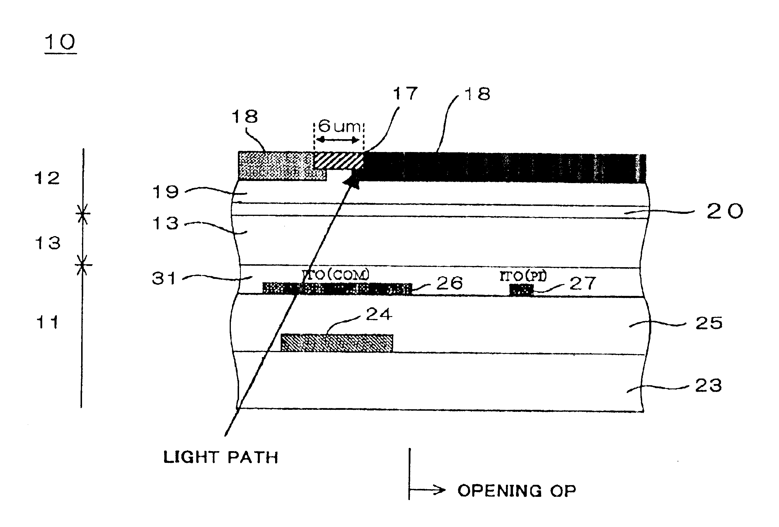
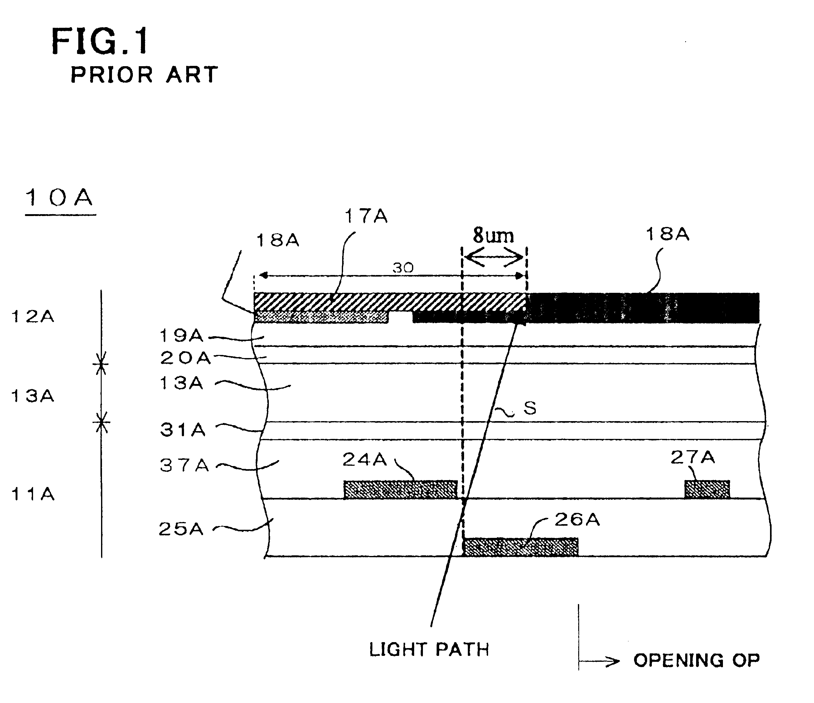
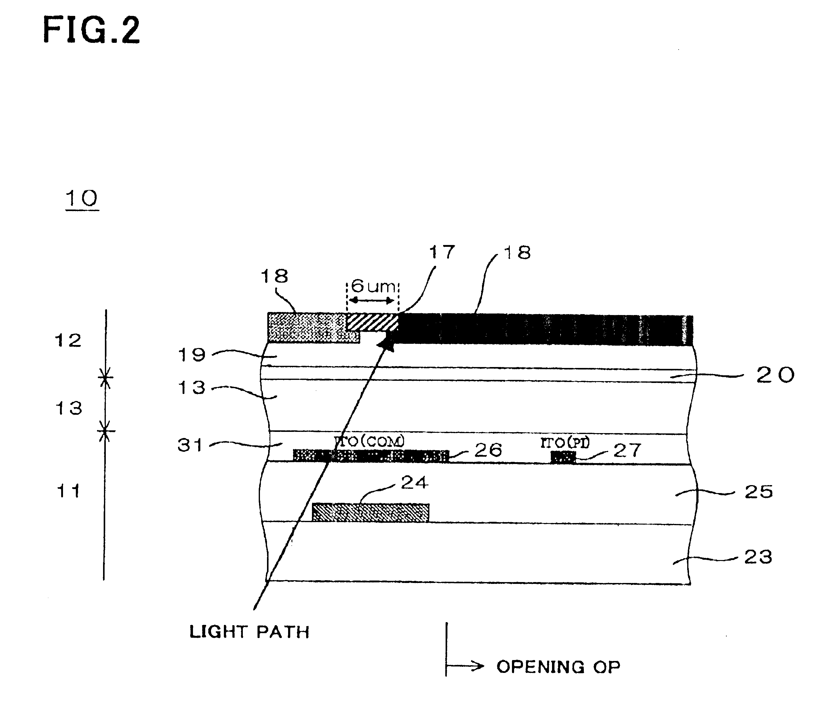
[0278]FIGS. 4, 5 and 6 illustrate an in-plane switching mode active matrix type liquid crystal display device in accordance with the first embodiment of the present invention. FIG. 4 is a plan view of the liquid crystal display device 10 in accordance with the first embodiment, FIG. 5 is a cross-sectional view taken along the line V—V in FIG. 4, and FIG. 6 is a circuit diagram of a unit pixel.

[0279]As illustrated in FIG. 5, the liquid crystal display device 10 is comprised of an active device substrate 11, an opposing substrate 12, and a liquid crystal layer 13 sandwiched between the active device substrate 11 and the opposing substrate 12.

[0280]The opposing substrate 12 includes an electrically insulating transparent substrate 16, a black matrix layer 17 formed on a first surface of the electrically insulating transparent substrate 16 as a light-impermeable film, a color layer 18 formed on the first surface of the electrically insulating transparent substrate 16 s...

first example

[0435]FIGS. 33A to 33J are cross-sectional views of the liquid crystal display device 10, illustrating respective steps of the first example of the method of fabricating the liquid crystal display device 10 including the second interlayer insulating film 25 having a multi-layered structure of an inorganic film and an organic film.

[0436]First, as illustrated in FIG. 33A, a chromium layer as the first metal layer is formed on a glass substrate as the electrically insulating transparent substrate 22, and then, is patterned by photolithography and dry etching into the common electrode lines 26a and 26b and the scanning line 28 in both the common electrode line terminal 41e and the scanning line terminal 41c.

[0437]Though only the common electrode line 26b is illustrated in FIGS. 33A to 35H, the common electrode line 26a together with the common electrode line 26b will be explained hereinbelow, because the common electrode line 26a is formed together with the common electrode line 26b.

[...

second example

[0448]FIGS. 34A to 34I are cross-sectional views of the liquid crystal display device 10, illustrating respective steps of the second example of the method of fabricating the liquid crystal display device 10 including the second interlayer insulating film 25 comprised singly of an organic film.

[0449]First, as illustrated in FIG. 34A, a chromium layer as the first metal layer is formed on a glass substrate as the electrically insulating transparent substrate 22, and then, is patterned by photolithography and dry etching into the common electrode lines 26a and 26b and the scanning line 28 in both the common electrode line terminal 41e and the scanning line terminal 41c.

[0450]Then, as illustrated in FIG. 34B, the first interlayer insulating film 23 is formed all over the transparent substrate 22, covering the common electrode lines 26a and 26b and the scanning line 28 therewith. The first interlayer insulating film 23 has a multi-layered structure of a silicon dioxide (SiO2) film and ...


PUM

PropertyMeasurementUnit
widthaaaaaaaaaa
thicknessaaaaaaaaaa
widthaaaaaaaaaa

Abstract

An in-plane switching mode active matrix type liquid crystal display device includes a first substrate, a second substrate located opposing the first substrate, and a liquid crystal layer sandwiched between the first and second substrates. The first substrate includes a thin film transistor, a pixel electrode each associated to a pixel to be driven, a common electrode to which a reference voltage is applied, data lines, a scanning line, and common electrode lines. Molecular axes of liquid crystal are rotated in a plane parallel with the first substrate by an electric field substantially parallel with a plane of the first substrate to thereby display certain images. The common electrode is composed of transparent material, and are formed on a layer located closer to the liquid crystal layer than the data lines. The common electrode entirely overlaps the data lines except an area where the data lines are located in the vicinity of the scanning line. The liquid crystal display device further includes a light-impermeable layer in an area where the common electrode entirely overlaps the data lines. The light-impermeable layer is comprised of a black matrix layer having a width smaller than a width of the common electrode.

Description

BACKGROUND OF THE INVENTION[0001]1. Field of the Invention[0002]The invention relates to a liquid crystal display device and a method of fabricating the same, and more particularly to an in-plane switching mode active matrix type liquid crystal display device and a method of fabricating the same.[0003]2. Description of the Related Art[0004]A liquid crystal display device may be grouped into two types, one of which the molecular axes of aligned liquid crystal molecules are rotated in a plane perpendicular to a substrate to display a certain image, and the other of which the molecular axes of aligned liquid crystal molecules are rotated in a plane parallel with a substrate to display a certain image.[0005]A typical one in the former type is a twisted nematic (TN) mode liquid crystal display device, and the latter type is called an in-plane switching (IPS) mode liquid crystal display device.[0006]Since a viewer looks only at a direction in which minor axes of liquid crystal molecules e...

Claims


Application Information

Patent Timeline
Patent Type & Authority Patents(United States)
IPC IPC(8): G02F1/13G02F1/1343G02F1/1335G02F1/1362G02F1/1337G02F1/1368G09F9/30G09F9/35H01L21/336H01L29/786
CPCG02F1/134363G02F1/133512G02F1/136213G02F1/136227G02F1/1343
Inventor NISHIDA, SHINICHIMATSUMOTO, KIMIKAZUHANNUKI, TAKAHISAITAKURA, KUNIMASA
Owner NEC LCD TECH CORP
Why Eureka
Try Eureka