Micromachined fiber optic sensors

a fiber optic sensor and micromachined technology, applied in the field of microoptic sensors, can solve problems such as limiting the temperature of operation of sensors

Inactive Publication Date: 2005-08-02
CINCINNATI UNIV OF
View PDF4 Cites 36 Cited by
  • Summary
  • Abstract
  • Description
  • Claims
  • Application Information

AI Technical Summary

Benefits of technology

[0005]This invention uses metal micro-electro-mechanical-systems (MEMS) and micro-optical-electro mechanical systems (MOEMS) including manufacturing components of micro-optic devices by photolithographic methods. In addition, a variety of substrates may be used, and the substrate material can be tailored to reduce costs and provide additional stability.
[0006]Optically interrogated pressure sensors have been demonstrated in various configurations using microelectromechanical systems (MEMS) technology [1-6]. In one embodiment, this technology is effective for pressure sensing because the small and precise sizes of sensing elements results in considerable flexibility in choosing pressure response ranges, bandwidth, and sensitivity. The use of MEMS technology is also advantageous because of the potential for economical manufacturing. Optical interrogation of these sensing elements presents an opportunity to extend use of these sensors to harsh environments in which electronics cannot operate. More specifically, optical interrogation is advantageous since it is superior to electrical interrogation in harsh environments, such as high temperature, vibration, EM interference, and dust. Traditional sensor configurations consist of a micromachined MEMS sensor structure and an appropriately aligned and fixed optical fiber for optical interrogation (FIG. 1(a)). Packaging of these sensors usually involves using adhesives that may limit the temperature of operation of the sensors.
[0007]The present invention is a novel MEMS sensors fabricated directly on an optical fiber end face. This configuration eliminates the need for adhesives in packaging and as a result, the temperature of operation of the sensor will be approximately that of the optical fiber. A unique feature of this proposed sensor is that processing is done on a commercial optical fiber as opposed to a wafer. The sensor configuration involves anodic bonding of a piece of an extremely thin silicon wafer onto the fiber end face. In one embodiment, the thin silicon is bonded over a cavity etched in the central portion of the fiber end face (FIG. 1(b)). The final device diameter is thus generally approximately the same or smaller than that of the optical fiber.
[0008]Due to their small size and the optical interrogation method, multiplexed arrays of such sensors can provide sensor maps with high spatial resolution.
[0009]The present invention provides for the fabrication of a novel optically-interrogated, microelectromechanical system (MEMS) sensors in which the entire MEMS structure is fabricated directly on an optical fiber. A new micromachining process for use on a flat fiber end face that includes photolithographic patterning, wet etching of a cavity, and anodic bonding of a silicon diaphragm is utilized. Generally, the sensor is made using multimode optical fibers having a diameter from about 10 μm to about 1000 μm, preferably from about 200 μm to about 400 μm. In a configuration as a pressure sensor fabricated on an optical fiber, it has been tested displaying an approximately linear response to static pressure (0-80 psi). This sensor is expected to find application in situations where small size is advantageous and where dense arrays may be useful.

Problems solved by technology

Packaging of these sensors usually involves using adhesives that may limit the temperature of operation of the sensors.

Method used


Image

  • Micromachined fiber optic sensors
  • Micromachined fiber optic sensors
  • Micromachined fiber optic sensors

Examples


example 1

Pressure Sensor Configuration and Fabrication

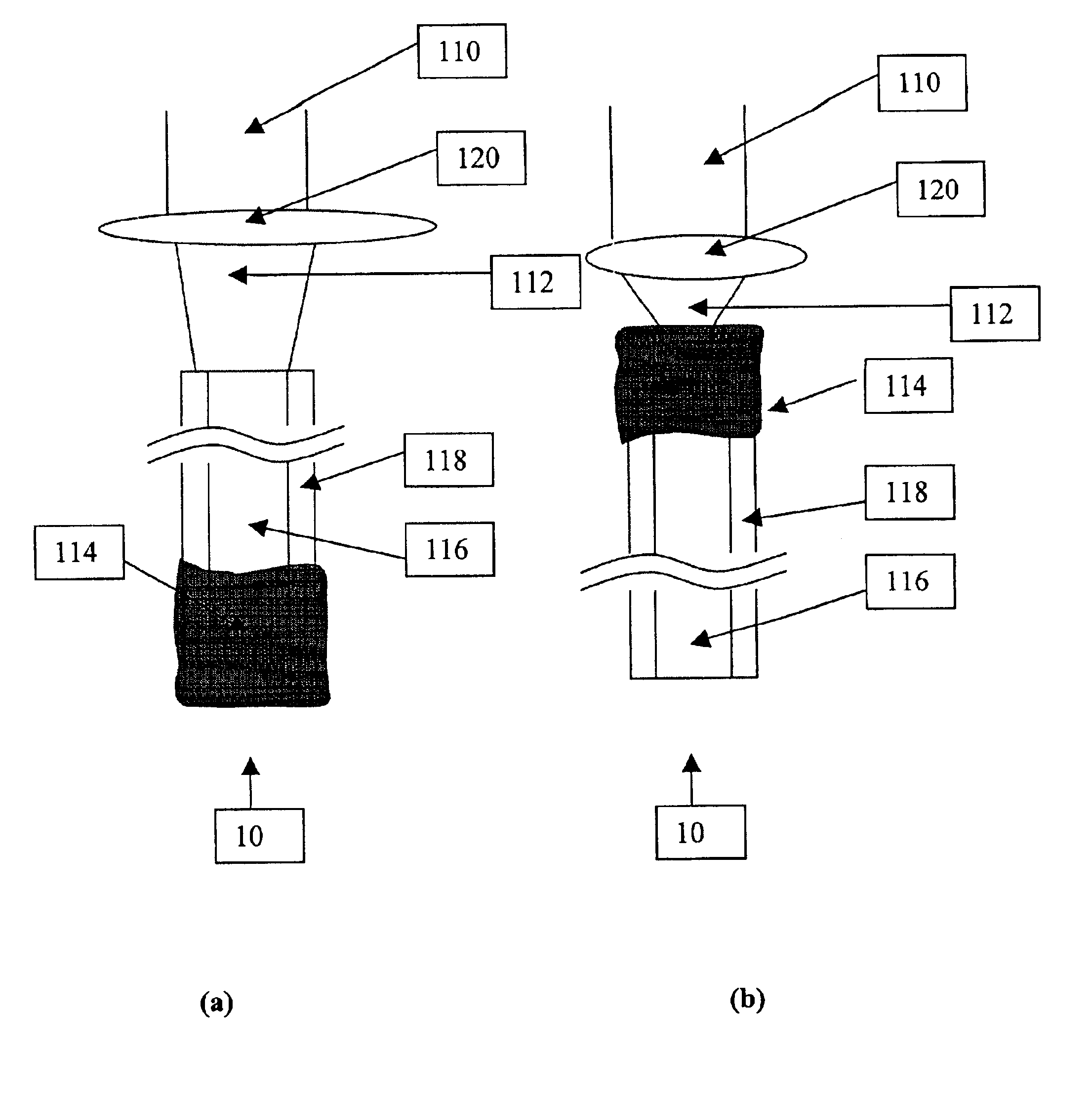
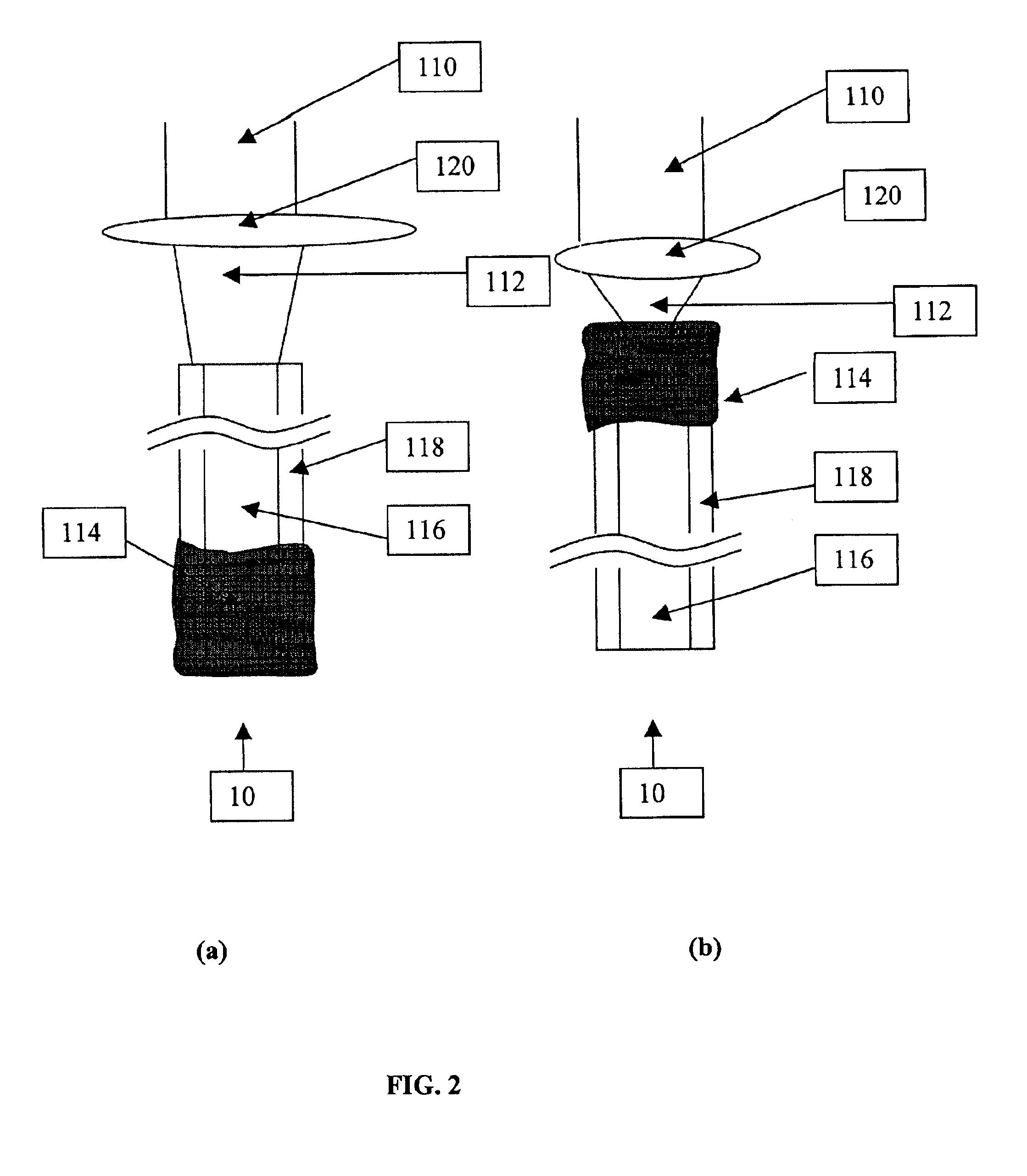
[0049]The configuration of the Fabry-Perot interferometric optical fiber pressure sensor reported here is shown in FIG. 1(b). The silicon diaphragm 12 and the cavity-fiber interface act as reflectors forming a Fabry-Perot interferometer. Pressure causes the diaphragm 12 to move, thus changing the Fabry-Perot reflectivity, and allowing measurement of pressure. The optical fibers 10 used for the fabrication are generally borosilicate multimode glass fibers (Techman International Corporation Inc.; the index of refraction of borosilicate glass is 1.5098 at 850 nm).

[0050]Optic fibers are generally used with cladding diameters of from about 1 μm to about 5000 μm and are preferably from about 2 μm to about 500 μm. For example, the diameter of the core will determine whether the fiber optic is “single mode” or “multimode”. The terms single mode and multimode refer to the dimensional orientation of rays propagating through the fiber. Single mode f...

example 2

Temperature Sensor Configuration

[0066]The temperature sensor is achieved by anodically bonding ultra-thin crystalline silicon onto a fiber end face (the figure above). Thin-film based temperature sensors have been realized in a number of ways including sputter-deposited semiconductor [6] and dielectric [7] materials. For effective operation the thickness of the silicon film of these Fabry-Perot interferometer based sensors usually falls within the range of 0.8 μm to 4.3 μm [6]. Greater sensitivity is obtained at the high end of this range; however, film-nonuniformity, and stress have been found to impose an upper thickness limit of about 2 μm for sputter-deposited semiconductors. In this study we used the anodic bonding method to chemically bond ultra-thin crystalline silicon onto fiber end faces; this enables achieving a thicker crystalline silicon layer on the fiber end face. As a result, a higher sensitivity can be expected. Further, the use of crystalline silicon with proper enc...


PUM

PropertyMeasurementUnit
thicknessaaaaaaaaaa
thicknessaaaaaaaaaa
thicknessaaaaaaaaaa

Abstract

A novel fiber optic sensor configuration whose diameter is the same as that of the optical fiber on which it is directly fabricated is introduced. A simple MEMS-compatible fabrication process to accomplish micromachining on the fiber end face has been developed and is detailed. This sensor configuration significantly reduces the size of the sensor and makes the packaging simple and adhesive free. The micromachining process of the present invention also provides for the fabrication of arrays of sensors that would provide two dimensional maps with high spatial resolution of at least one of acoustical vibration, mechanical vibration, pressure, temperature, acceleration, electrostatic fields, magnetic fields or combinations thereof.

Description

[0001]This application claims the benefit of U.S. Provisional Patent Application Ser. No. 60 / 274,513, filed Mar. 9, 2001, which application is hereby incorporated by reference in its entirety.BACKGROUND OF THE INVENTION[0002]The present invention relates to micro-optic sensors used for transmitting pressure sensor signals by optical fibers. More particularly, the invention pertains to fiber optic sensors using silicon structures anodically bonded to the central portion of the fiber end face for detection of at least one of acoustical vibration, mechanical vibration, pressure, temperature, acceleration, electrostatic fields and magnetic fields. The micromachining process of the present invention also provides for the fabrication of arrays of sensors that would provide two dimensional maps with high spatial resolution of at least one of acoustical vibration, mechanical vibration, pressure, temperature, acceleration, an electrostatic field magnetic field or combinations thereof.[0003]O...

Claims


Application Information

Patent Timeline
Patent Type & Authority Patents(United States)
IPC IPC(8): G01L9/00G01D5/26G02B6/26
CPCG01D5/268G01L9/0079G02B6/262
Inventor BOYD, JOSEPH T.ABEYSINGHE, DON C.DASGUPTA, SAMHITAJACKSON, HOWARD E.
Owner CINCINNATI UNIV OF
Why Eureka
Try Eureka