Method for manufacturing semiconductor device

Inactive Publication Date: 2005-08-09
STMICROELECTRONICS SRL +1
View PDF3 Cites 5 Cited by
  • Summary
  • Abstract
  • Description
  • Claims
  • Application Information

AI Technical Summary

Benefits of technology

[0006]A method for manufacturing a semiconductor device is disclosed that is capable of securing the stability

Problems solved by technology

However, after the polishing process, an insulator film is over-dished due to differences of an etching rate between the insulator film deposited for insulating of the word lines and a poly silicon film for a landing plug (hereinafter also referred to as a “LP”).
The aforementioned slurry residues are mostly composed of metal materials having electric c

Method used


Image

  • Method for manufacturing semiconductor device
  • Method for manufacturing semiconductor device
  • Method for manufacturing semiconductor device

Examples


Embodiment Construction

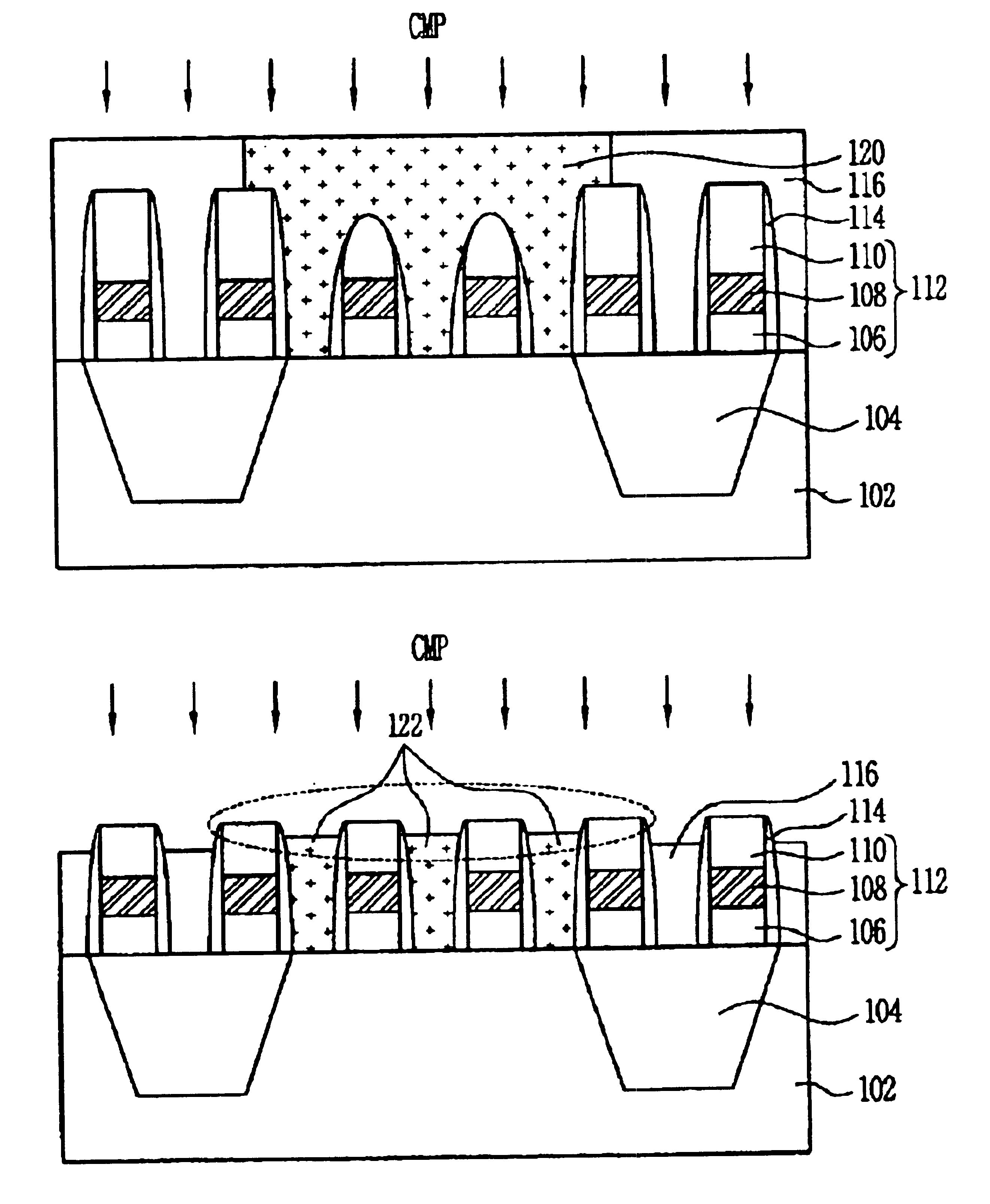
[0012]Now certain preferred embodiments will be described with reference to the accompanying drawings.

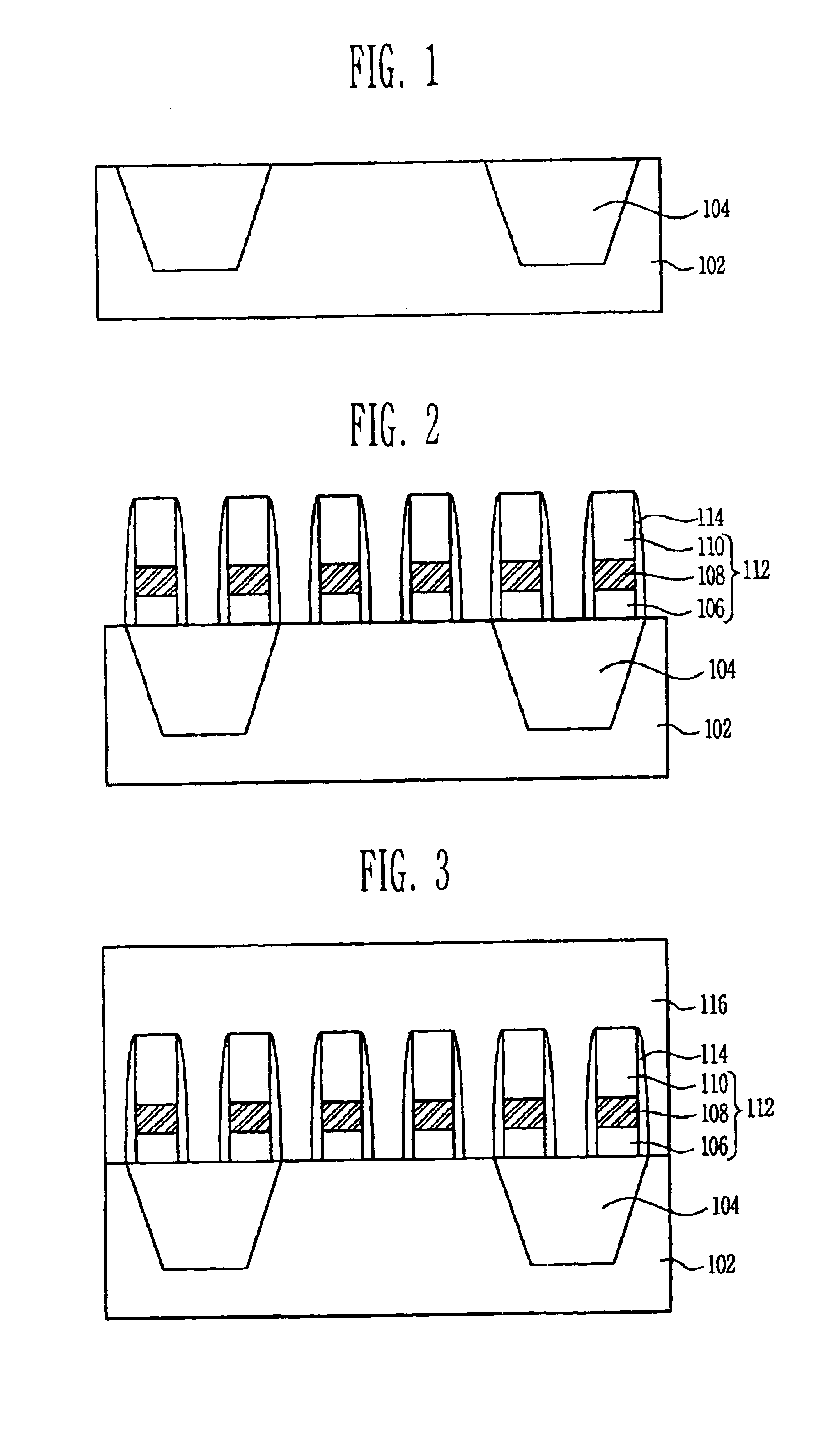
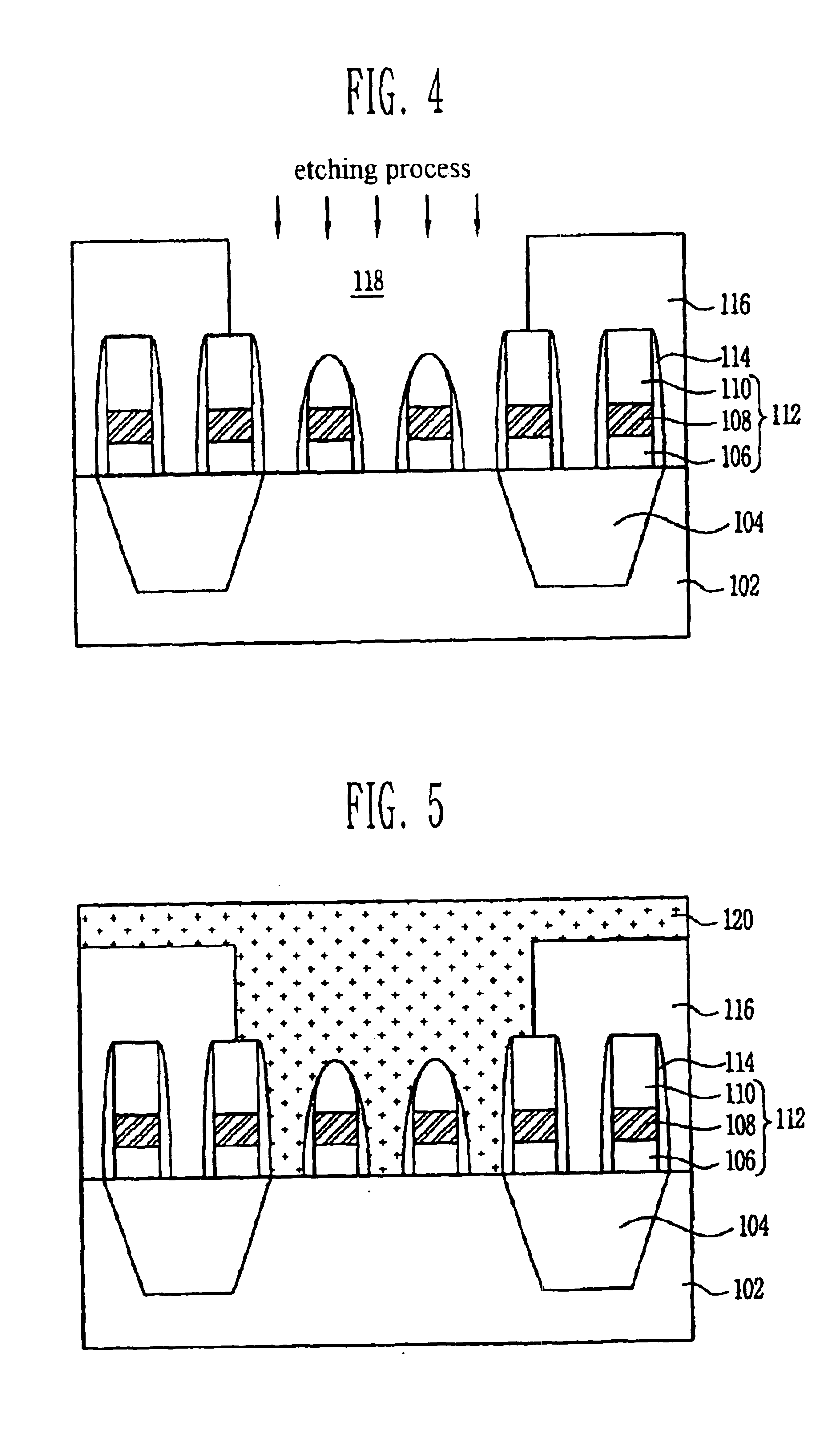
[0013]Referring to FIG. 1, a semiconductor substrate 102 is provided, wherein the semiconductor substrate is defined as an active region and a field region and it is cleaned by the cleaning process using at least one of diluted HF (DHF), SC-1, and BOE. A field oxide film 104 is formed in the field region of the semiconductor substrate 102. The field oxide film 104 is formed to have a trench structure using shallow trench isolation (STI) process or LOCal oxidation of silicon (LOCOS) process.

[0014]Referring to FIG. 2, a number of gate electrodes 112 (hereinafter, “word lines”) are formed on the semiconductor substrate 102 including the active region and the field region, which is the field oxide film 104. Word lines 112 include the gate oxide film 106, the gate layer 108, and a hard mask layer 110. The gate layer 108 includes at least one of the poly silicon films or of the doped poly...


PUM


Abstract

A method of manufacturing a semiconductor device capable of polishing evenly and separating the adjacent word lines by performing the flattening process using slurry with a doping material added during the polishing process.

Description

BACKGROUND[0001]1. Technical Field[0002]A method for manufacturing a semiconductor device is disclosed, that is capable of securing the stability in a polishing process for forming a landing plug.[0003]2. Discussion of Related Art[0004]Generally, a polishing process is performed for an electric isolation of word lines at the time of manufacturing a semiconductor. However, after the polishing process, an insulator film is over-dished due to differences of an etching rate between the insulator film deposited for insulating of the word lines and a poly silicon film for a landing plug (hereinafter also referred to as a “LP”). Thereby, slurry residues generated during the polishing process become to remain on an upper face of the insulator film over-dished. The aforementioned slurry residues are mostly composed of metal materials having electric conductivity, and they come to remain as they are because it is difficult to remove them through the following cleaning process. The residues, a...

Claims


Application Information

Patent Timeline
IPC IPC(8): H01L21/28H01L21/304H01L21/31H01L21/3105H01L21/3205H01L21/321H01L21/461H01L21/4763H01L21/768H01L21/8242H01L27/108
CPCH01L21/31053H01L21/3212H01L21/7684H10B12/05H01L21/304
Inventor SONG, YOUNG TAEK
Owner STMICROELECTRONICS SRL
Why Eureka
Try Eureka