
Dual function array feature for CMP process control and inspection

a technology of process control and array feature, applied in the direction of individual semiconductor device testing, semiconductor/solid-state device testing/measurement, instruments, etc., can solve the problems of increasing equipment expenses, slowing manufacturing throughput during the fabrication process, and increasing the cost of the fabrication process, so as to achieve rapid and simple cmp process control, reduce the cost of manufacturing, and improve the effect of manufacturing efficiency

Inactive Publication Date: 2005-08-16
WESTERN DIGITAL TECH INC
View PDF27 Cites 0 Cited by
  • Summary
  • Abstract
  • Description
  • Claims
  • Application Information

AI Technical Summary

Benefits of technology

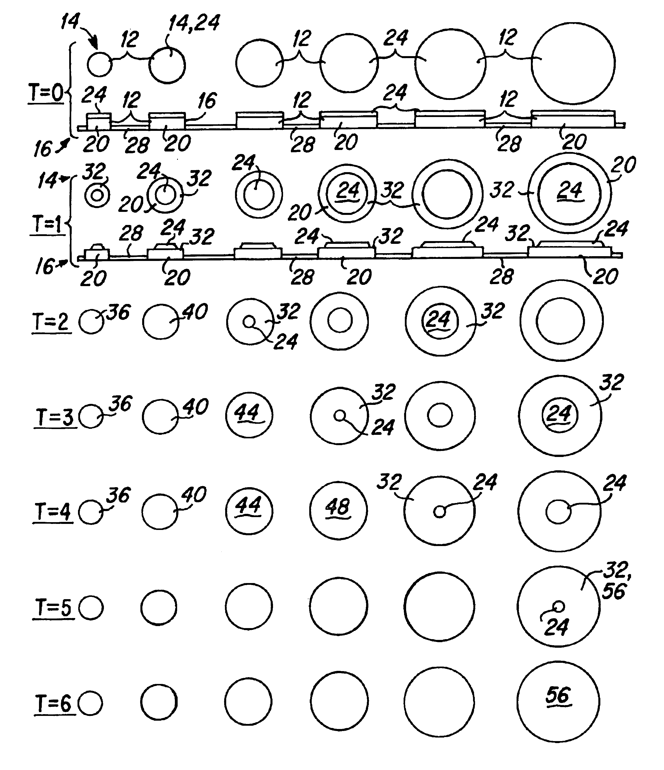
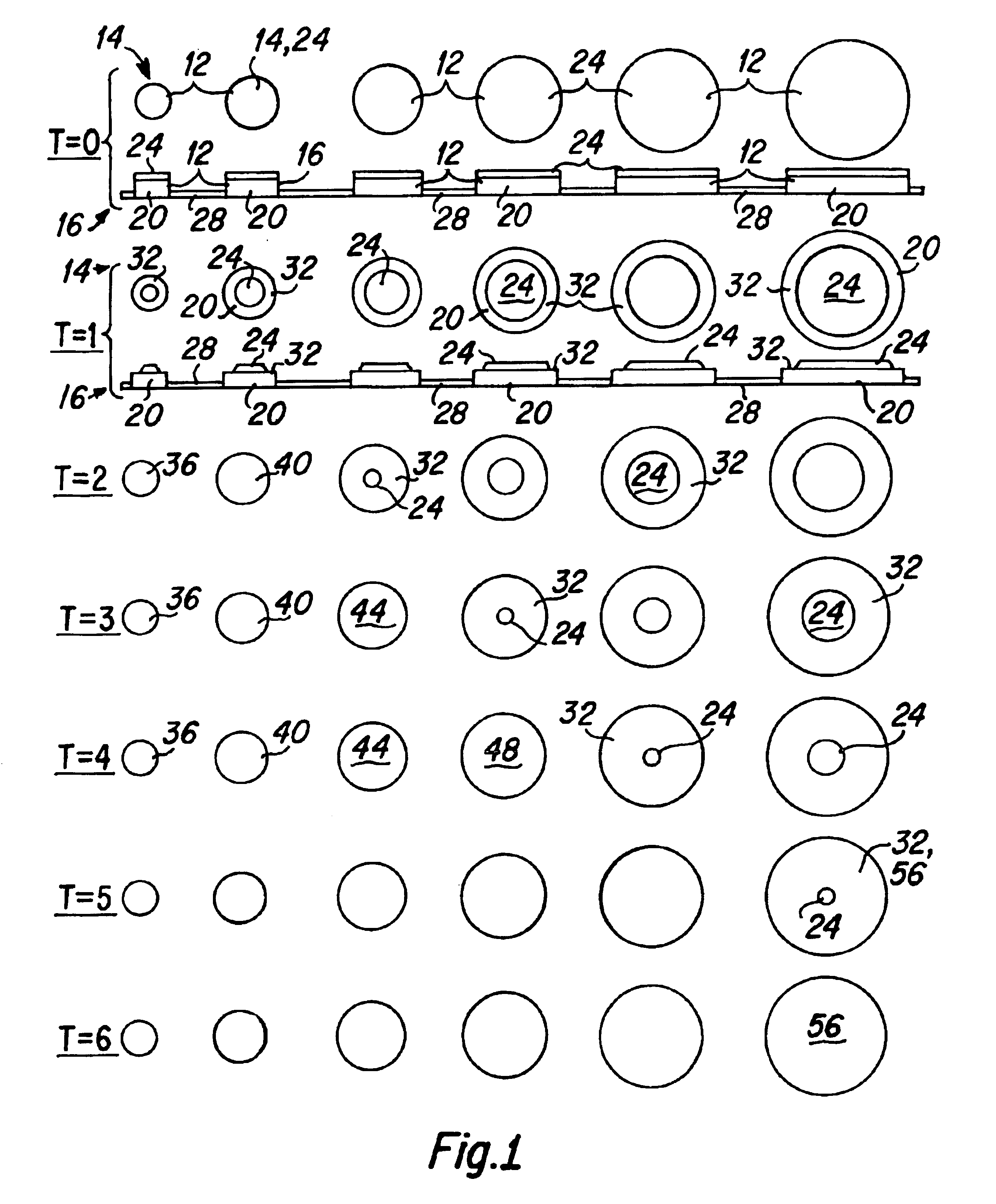
[0008]As a result, CMP process control of delicate features that are too small to be viewed utilizing an optical microscope, can be obtained by fabricating arrays that include a plurality of projecting test features which when viewed together in an array are visible utilizing the dark field optical microscope. CDSEM methodology may also be used as a complimentary tool for further process diagnostic and fine tuning. The overall benefit of this method is that it combines a quick and simple CMP process control at an operator level utilizing a dark field optical microscope, and a precise CMP process engineering level fine tuning utilizing a CDSEM when it is needed.
[0009]It is an advantage of the CMP control process of the present invention that a relatively inexpensive optical microscope can be utilized to provide CMP process control of delicate features that are too small to be seen utilizing an optical microscope.
[0010]It is another advantage of the CMP control process of the present invention that the polishing of features that are only a fraction of a micron in size can be controlled utilizing a conventional optical microscope.
[0011]It is a further advantage of the CMP process control of the present invention that a plurality of arrays can be created on a wafer surface that provide a time intervalled polishing indication.
[0012]It is yet another advantage of the CMP control process of the present invention that a more rapid, less expensive method for polishing control is provided.
[0013]It is yet a further advantage of the CMP control process of the present invention that it combines a quick and simple CMP process control at an operator level utilizing optical microscopes, and a precise CMP process engineering fine tuning utilizing a CDSEM when it is needed.

Problems solved by technology

As is well known to those skilled in the art, where a CMP step is undertaken above delicate structures, such as the sensor layer structure of a read head portion of a magnetic head, accurate process control must be maintained, such that the CMP step is conducted for sufficient time to remove the unwanted surface layers or features, while not overpolishing and removing the desired delicate structures.
The use of the CDSEM for process control increases equipment expenses and is time consuming, and therefore slows manufacturing throughput during the fabrication process.
Additionally, because skilled operators are required to operate a CDSEM properly, the expense of the fabrication process is increased.

Method used


Image

  • Dual function array feature for CMP process control and inspection
  • Dual function array feature for CMP process control and inspection
  • Dual function array feature for CMP process control and inspection

Examples


Embodiment Construction

[0023]Chemical mechanical polishing (CMP) steps are commonly undertaken during the fabrication of thin film devices such as magnetic heads for hard disk drives. Where delicate structures are involved, such as the read sensors of a giant magnetoresistive read head, the CMP step must be closely monitored to remove the unwanted material while not also removing the desired read head structure. The process control for such a CMP step is generally conducted using a critical dimension scanning electron microscope (CDSEM). A skilled operator is generally required to operate the CDSEM and significant time is involved in this process control step. The present invention allows the utilization of an optical microscope to control the CMP step, such that a less trained operator can conduct process control, and less time and expense is involved in controlling the CMP step.

[0024]As will be understood from reading this detailed description, the present invention utilizes grouped arrays of small proj...


PUM


Abstract

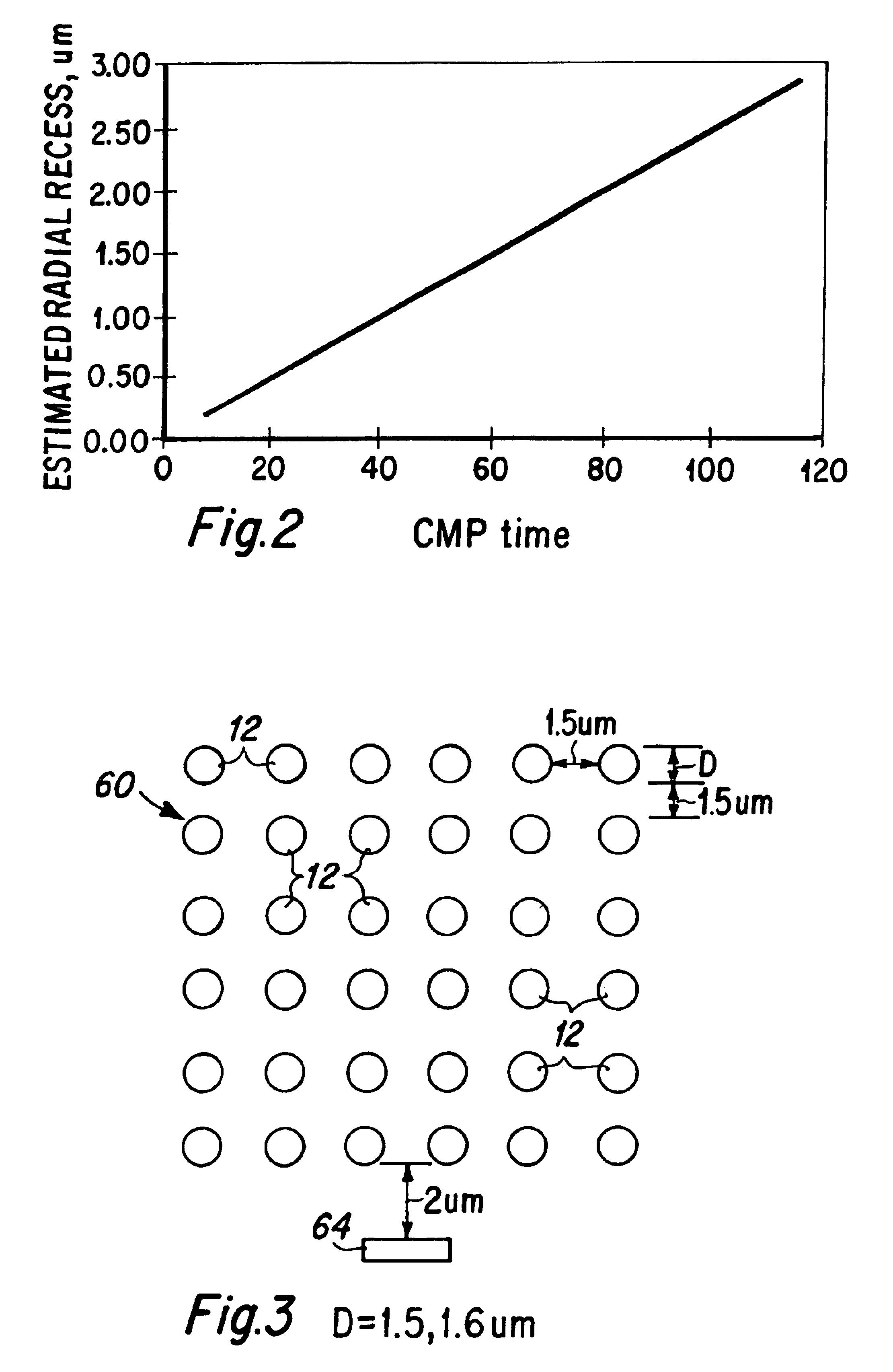
CMP process control array groups are fabricated upon the surface of the wafer for viewing through an optical microscope. The array groups include a plurality of test arrays, where each array includes a plurality of projecting test features. Each of the projecting test features are formed with the same projecting height and have a hard upper surface layer, such as diamond-like-carbon (DLC). All of the projecting test features within an array are formed with the same diameter, and the diameter of projecting test features of a particular array differs from the diameter of projecting test features in another array. The diameters are chosen such that the DLC surface is removed in specifically designed time increments, such as 5 seconds, from array to array, where projecting test features with the DLC surface removed appear as bright white, while the arrays with test features that retain some DLC surface are significantly darker.

Description

BACKGROUND OF THE INVENTION[0001]1. Field of the Invention[0002]The present invention relates generally to chemical mechanical polishing (CMP) process control, and more particularly to a CMP process control feature suitable for both optical microscope inspection and critical dimension scanning electron microscope inspection and measurement.[0003]2. Description of the Prior Art[0004]In the fabrication of thin film devices such as magnetic heads for hard disk drives, one or more chemical mechanical polishing (CMP) steps are often undertaken to remove portions of existing surface features and obtain a generally flat, smooth surface upon which to fabricate further thin film layers and structures. As is well known to those skilled in the art, where a CMP step is undertaken above delicate structures, such as the sensor layer structure of a read head portion of a magnetic head, accurate process control must be maintained, such that the CMP step is conducted for sufficient time to remove th...

Claims


Application Information

Patent Timeline
Patent Type & Authority Patents(United States)
IPC IPC(8): H01L21/00H01L23/544
CPCH01L22/34
Inventor HWU, JUSTIN JIA-JENLEONG, THOMAS L.
Owner WESTERN DIGITAL TECH INC
Learn More