Supercharge Your Innovation With Domain-Expert AI Agents!

Etching a metal hard mask for an integrated circuit structure

a metal hard mask and integrated circuit technology, applied in the direction of basic electric elements, semiconductor/solid-state device manufacturing, electric apparatus, etc., can solve the problem that the chlorine-containing plasma that is typically used to etch the metal hard mask layer cannot be used in a medium-density tool used to etch the dielectric layer

Inactive Publication Date: 2005-08-16
LAM RES CORP
View PDF3 Cites 43 Cited by
  • Summary
  • Abstract
  • Description
  • Claims
  • Application Information

AI Technical Summary

Benefits of technology

[0014]Additionally, a method for etching a photoresist without affecting the metal hard mask layer is described. The method of et

Problems solved by technology

However, the chlorine-containing plasma that is typically used to etch the metal hard mask layer cannot be used in a medium-density tool used to etch the dielectric layer.

Method used


Image

  • Etching a metal hard mask for an integrated circuit structure
  • Etching a metal hard mask for an integrated circuit structure
  • Etching a metal hard mask for an integrated circuit structure

Examples


Embodiment Construction

[0022]In the following detailed description, reference is made to the accompanying drawings, which form a part of this application. The drawings show, by way of illustration, specific embodiments in which the invention may be practiced. It is to be understood that other embodiments may be utilized and structural changes may be made without departing from the scope of the present invention.

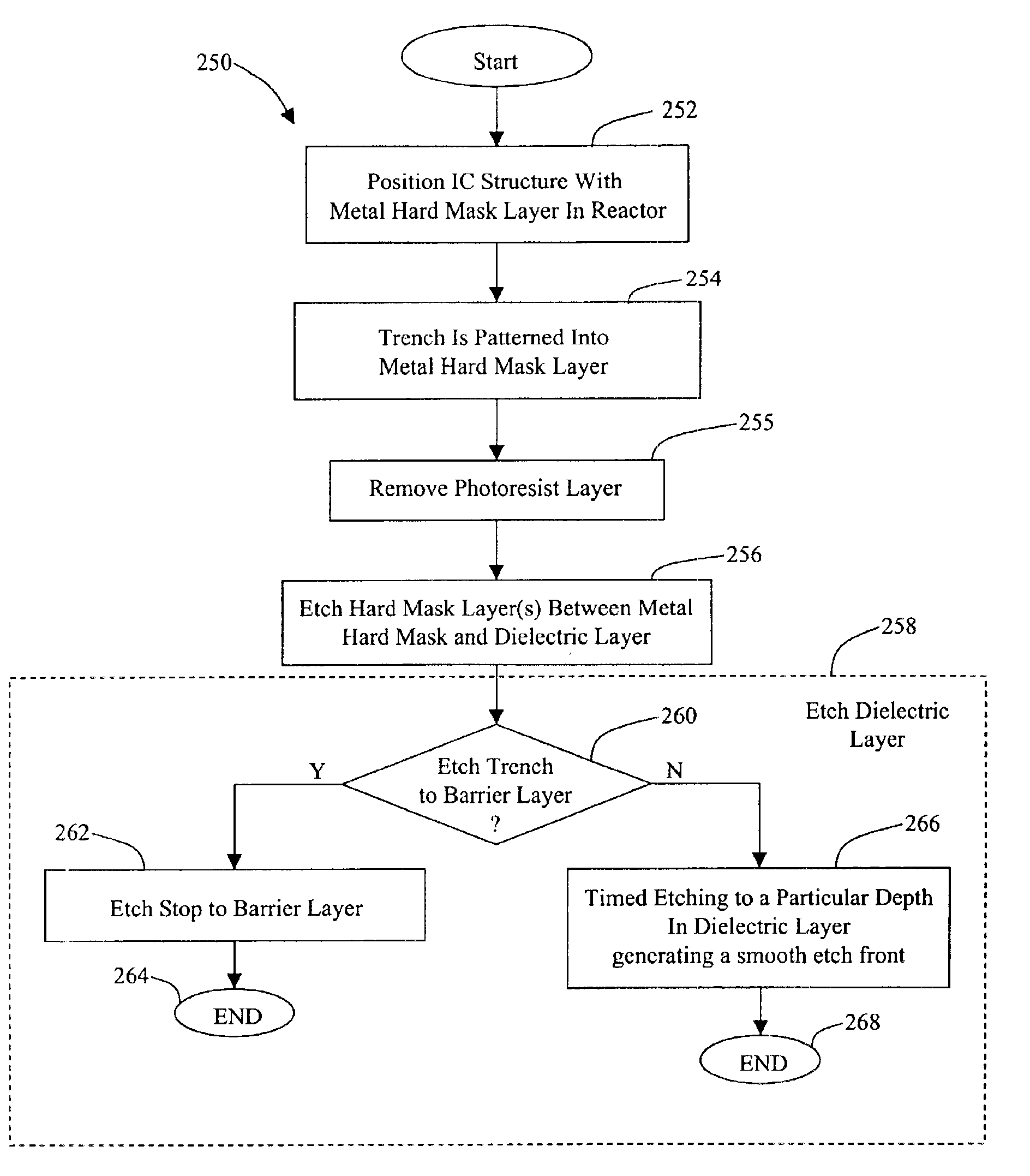
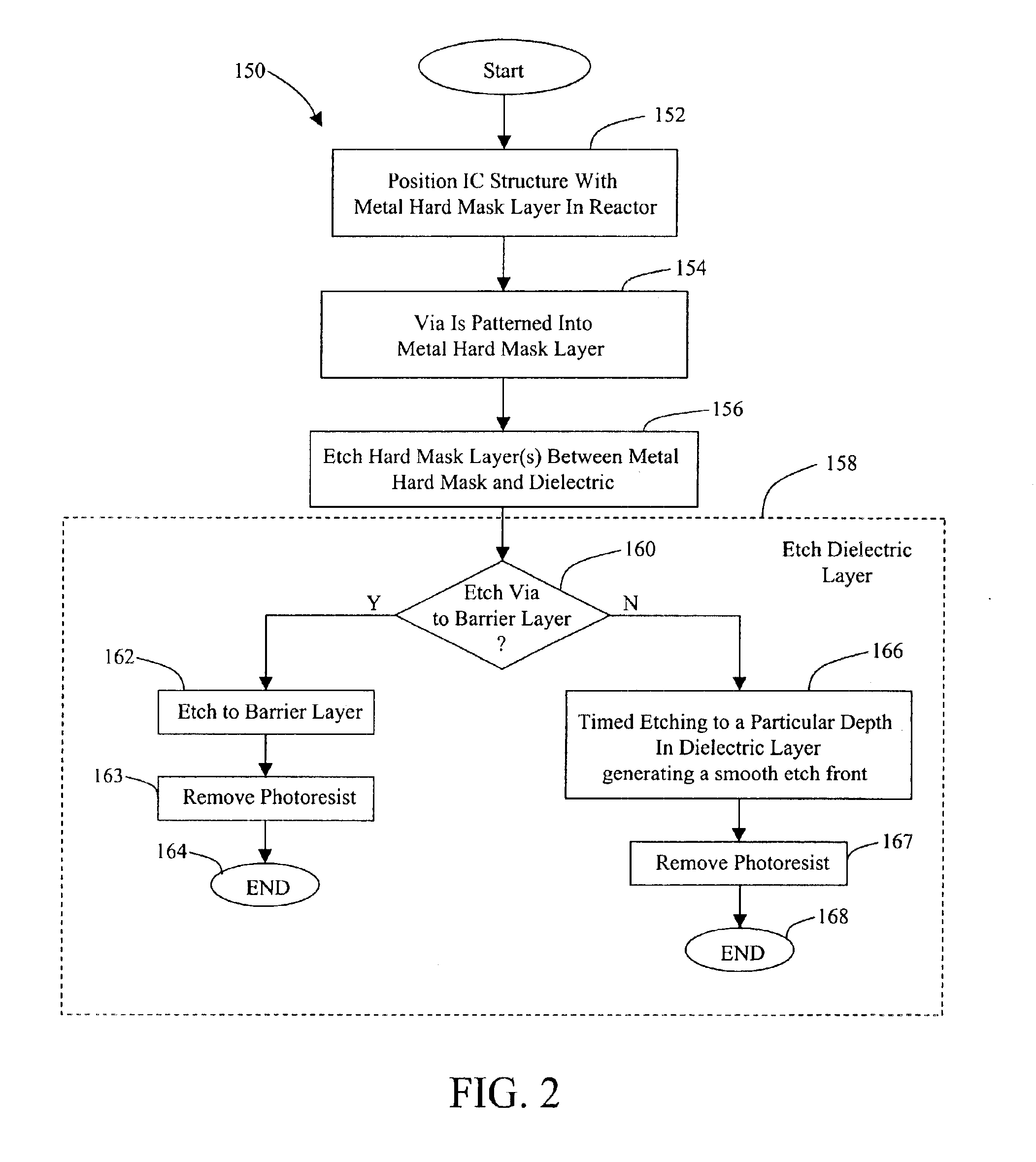
[0023]The present invention is related to the etching of a metal hard mask layer. It shall be appreciated by those of ordinary skill in the art that the method can be applied to the etching of “0.10 μm and beyond” features sizes including 0.07 μm feature sizes and any other feature size which is less than 0.10 μm. This description teaches a method for metal hard mask etching and a method for removing a photoresist layer. Finally, the resulting interconnect structure having a via opening and a trench opening is also described.

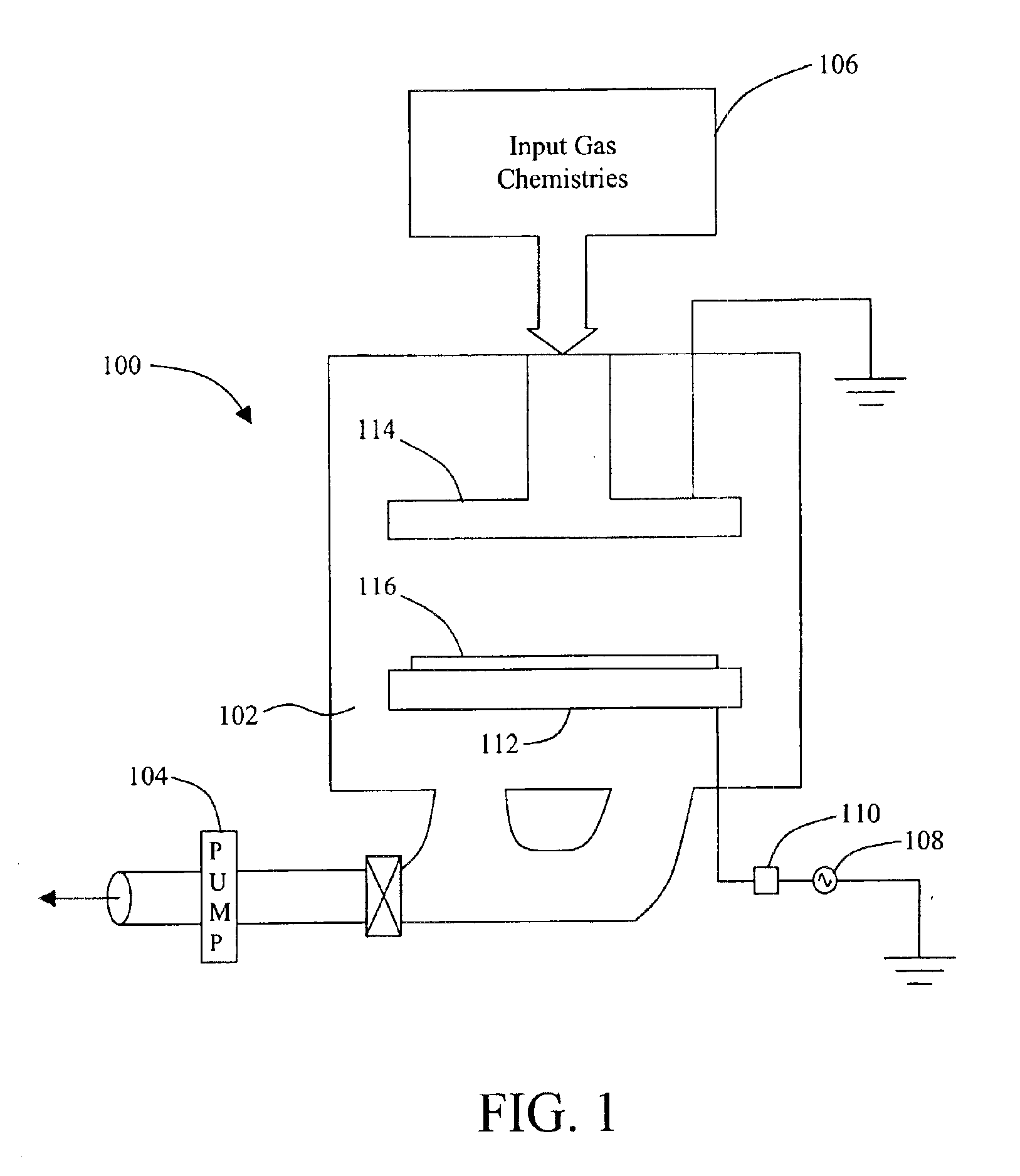
[0024]Referring to FIG. 1 there is shown an illustrative device for perfor...


PUM


Abstract

The invention is a method of etching an integrated circuit (IC) structure that includes a metal hard mask layer. The etching of the metal hard mask layer is performed by first feeding a gas mixture comprising a fluorine containing gas and oxygen (O2) gas to a reactor. The method then proceeds to generate a plasma that etches the metal hard mask layer. The method can be applied to either performing a via etch or a trench etch. Additionally, the invention teaches the removal of a photoresist layer without affecting the metal hard mask layer.

Description

BACKGROUND OF THE INVENTION[0001]1. Field of Invention[0002]The present invention relates to the etching of an integrated circuit structure. More particularly, the present invention describes etching an integrated circuit having a metal hard mask layer.[0003]2. Description of Related Art[0004]Metals such as Tantalum (Ta) and Titanium (Ti) and metallic compounds such as Tantalum Nitride (TaN) and Titanium Nitride (TiN) have been widely used in integrated circuit fabrication. More particularly, these metals and metallic compounds have been used as antireflective coatings or barrier layers.[0005]As IC manufacturing technology enters into 0.10 μm and beyond technology nodes, metals and metallic compounds are being investigated as a hard mask layer for a dielectric layer such as porous organo-silica-glass (pOSG).[0006]There are many well-known approaches to etching a metal hard mask. One well known method uses a high-density plasma reactor in conjunction with a chlorine-containing plasma...

Claims


Application Information

Patent Timeline
IPC IPC(8): H01L21/02H01L21/302H01L21/3213H01L21/768
CPCH01L21/32136H01L21/76802H01L21/76832
Inventor LI, SIYISADJADI, S.M. REGAKANG, SEAN S.LE, TRIYEN, BI-MINGBRIGGS, SCOTT
Owner LAM RES CORP
Features
  • R&D
  • Intellectual Property
  • Life Sciences
  • Materials
  • Tech Scout
  • Unparalleled Data Quality
  • Higher Quality Content
  • 60% Fewer Hallucinations
Learn More