

Multilayer printed wiring board and method of producing multilayer printed wiring board
a printing board and multi-layer technology, applied in the direction of printed circuit aspects, printed element electric connection formation, insulating substrate metal adhesion improvement, etc., can solve the problems of increasing the probability of generating defects, the inability to flatten and smooth a core substrate, and the disconnection of multi-layer resin insulating layers
- Summary
- Abstract
- Description
- Claims
- Application Information
AI Technical Summary
Benefits of technology
Problems solved by technology
Method used
Image

Examples
first embodiment
[0041]The embodiments of the present invention will be described hereinafter with reference to the accompanying drawings.
[0042]First, the constitution of a multi-layer printed circuit board according to the first embodiment of the present invention will be described with reference to FIG. 6 showing a longitudinal sectional view.
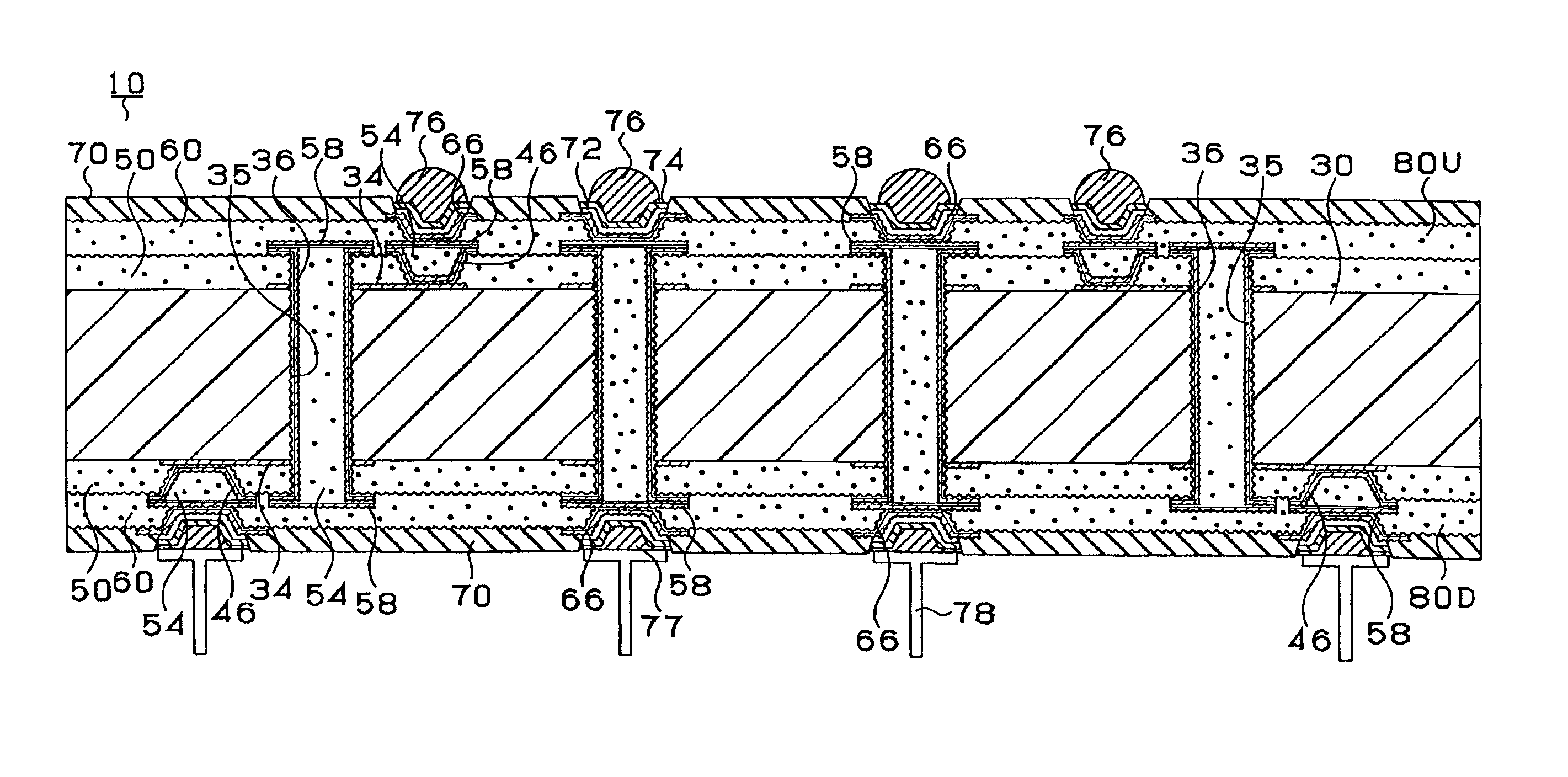
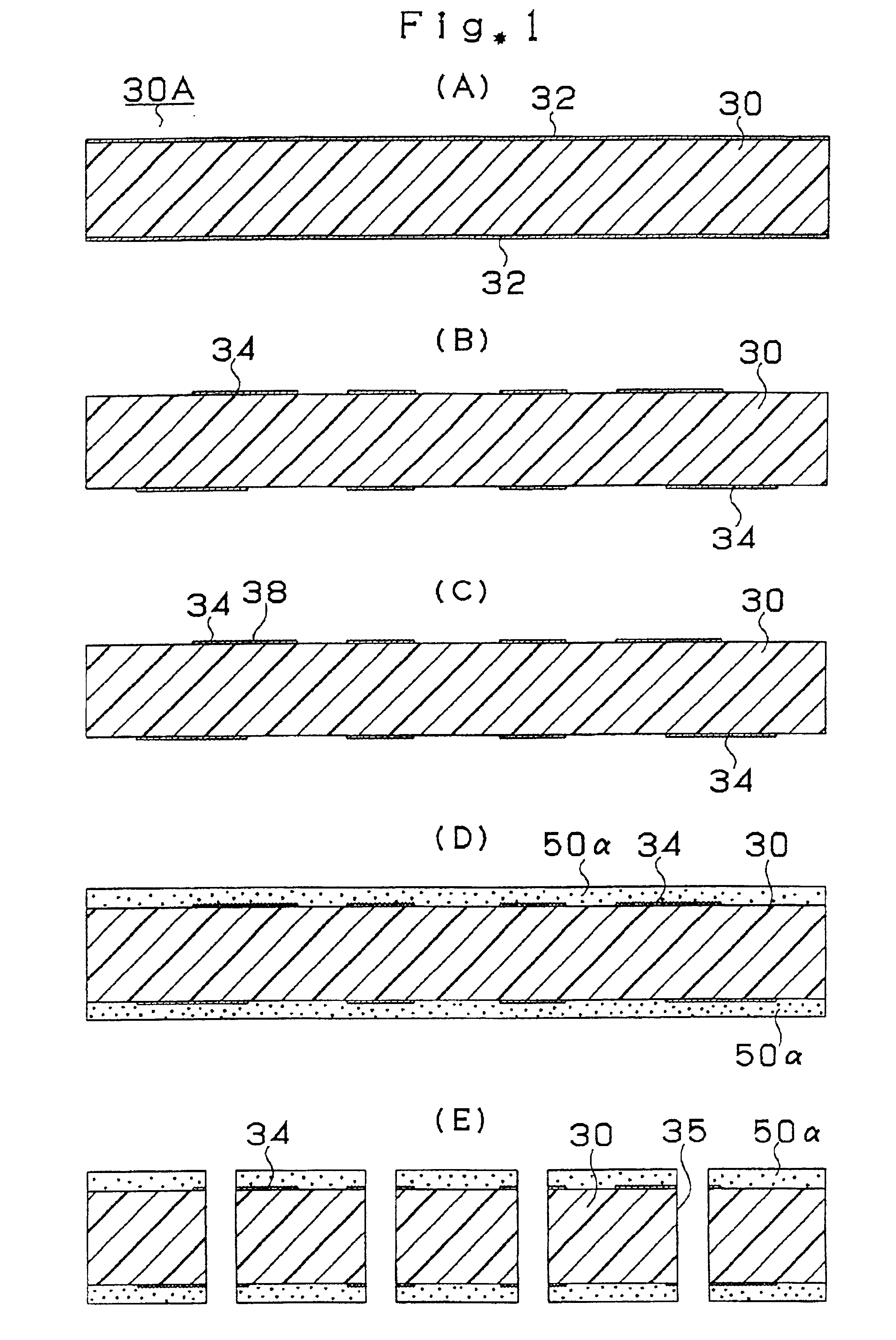
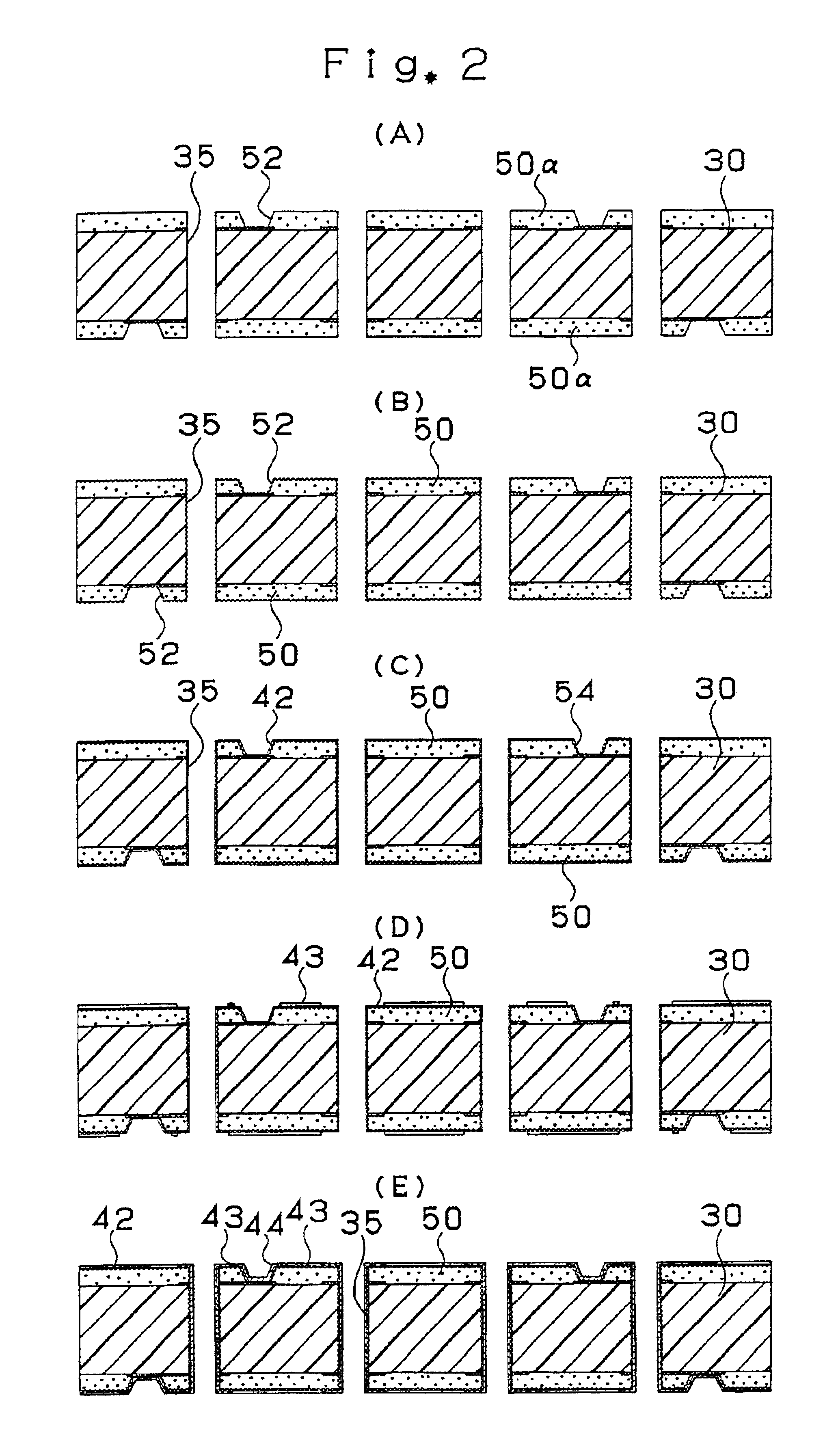
[0043]As shown in FIG. 6, a multi-layer printed circuit board 10 has a core substrate 30 having right and reverse sides on which buildup wiring layers 80U and 80D are formed, respectively. Each of the buildup wiring layers 80U and 80D consists of a lower interlayer resin insulating layer 50 in which via holes 46 are formed, an upper interlayer resin insulating layer 60 in which upper via holes 66 are formed, and a solder resist layer 70 formed on the upper interlayer resin insulating layer 60. A solder bump (external connection terminal) 76 for connecting the board 10 to an IC chip (not shown) is formed on each of the upper via holes 66 through the opening po...
second embodiment
[0142]The constitution of a printed circuit board according to the second embodiment of the present invention will be described hereinafter with reference to FIG. 13 which is a cross-sectional view of a printed circuit board 110.
[0143]The printed circuit board 110 consists of a core substrate 130 and buildup wiring layers 180A and 180B. Each of the build up wiring layers 180A and 180B consists of interlayer resin insulating layers 150 and 160. Via holes 146 and conductor circuits 145 are formed on the interlayer resin insulating layers 150. Via holes 166 and conductor circuits 165 are formed on the interlayer resin insulating layers 160. Solder resist layers 170 are provided on the respective interlayer resin insulating layers 160.
[0144]Next, description will be given to a method of manufacturing the printed circuit board according to the second embodiment of the present invention. Here, A. interlayer resin insulating films used for manufacturing the printed circuit board in the sec...
PUM
| Property | Measurement | Unit |
|---|---|---|
| thickness | aaaaa | aaaaa |
| thickness | aaaaa | aaaaa |
| thickness | aaaaa | aaaaa |
Abstract
Description
Claims
Application Information