Integrated circuits including insulating spacers that extend beneath a conductive line

a technology of integrated circuits and conductive lines, which is applied in the direction of semiconductor devices, semiconductor/solid-state device details, electrical apparatus, etc., can solve the problems of lowering the reliability of insulation, affecting the reliability of devices, and difficult to provide electrical insulation reliability, so as to achieve the effect of improving insulation reliability

Inactive Publication Date: 2005-08-16
SAMSUNG ELECTRONICS CO LTD
View PDF2 Cites 16 Cited by
  • Summary
  • Abstract
  • Description
  • Claims
  • Application Information

AI Technical Summary

Benefits of technology

[0015]Some embodiments of the present invention provide an integrated circuit device that includes an integrated circuit substrate, an insulating layer on the integrated circuit substrate, and a conductive line on the insulating layer. The conductive line includes a bottom adjacent the insulating layer, a top remote from the insulating layer and first and second sidewalls therebetween. An insulating spacer extends along the first and second sidewalls, and also extends along at least a portion of the bottom between the conductive line and the insulating layer. By providing an insulating spacer beneath at least a portion of the conductive line, insulation reliability may be improved even as the spacer may become narrower and / or the contact area may be enlarged.

Problems solved by technology

As integrated circuit devices become more highly integrated, the reliability of insulation between conductive line interconnections may impact the reliability of the devices.
Accordingly, it may be difficult to provide electrical insulation reliability between the bit line and the adjacent storage node contact pad.
However, if the contact area is increased, the insulation reliability may be lowered.
Accordingly, it may be difficult to decrease the contact resistance of the storage node contact pad without deteriorating the insulation reliability.

Method used


Image

  • Integrated circuits including insulating spacers that extend beneath a conductive line
  • Integrated circuits including insulating spacers that extend beneath a conductive line
  • Integrated circuits including insulating spacers that extend beneath a conductive line

Examples


Embodiment Construction

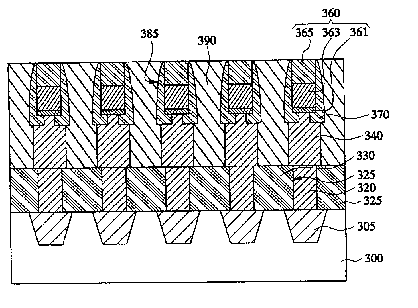
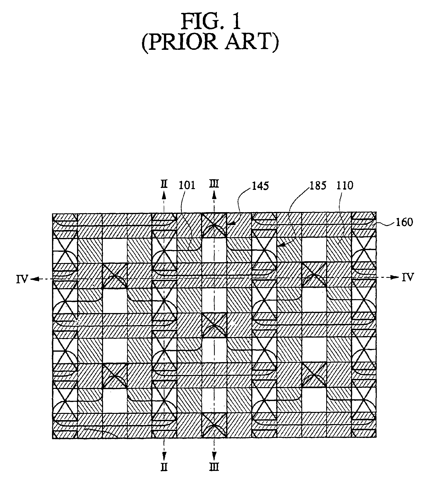
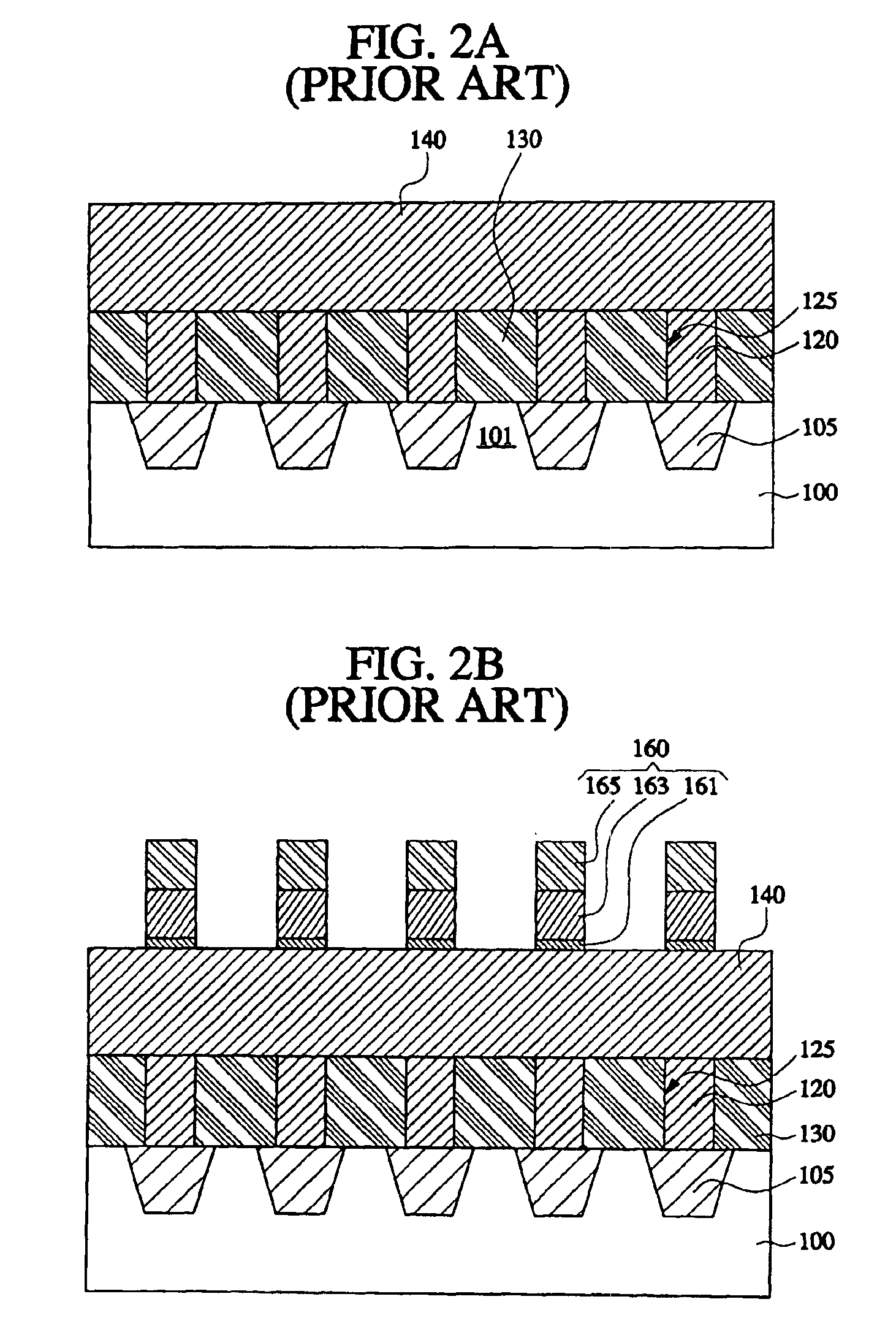
[0029]The present invention now will be described more fully hereinafter with reference to the accompanying drawings, in which embodiments of the invention are shown. This invention may, however, be embodied in many different forms and should not be construed as limited to the embodiments set forth herein. Rather, these embodiments are provided so that this disclosure will be thorough and complete, and will fully convey the scope of the invention to those skilled in the art. In the drawings, the size and relative sizes of layers and regions may be exaggerated for clarity. Moreover, each embodiment described and illustrated herein includes its complementary conductivity type embodiment as well. Like numbers refer to like elements throughout.

[0030]It will be understood that when an element such as a layer, region or substrate is referred to as being “on” another element, it can be directly on the other element or intervening elements may also be present. It will be understood that if ...


PUM


Abstract

Integrated circuit devices are fabricated by fabricating a conductive line on an insulating layer on an integrated circuit substrate. The conductive line includes a bottom adjacent the insulating layer, a top remote from the insulating layer and first and second sidewalls therebetween. An insulating spacer is formed to extend along the first and second sidewalls and to also extend along at least a portion of the bottom between the conductive line and the insulating layer. By providing an insulating spacer beneath at least a portion of the conductive line, insulation reliability may be improved even as the spacer may become narrower and / or the contact area may be enlarged.

Description

RELATED APPLICATION[0001]This application claims the benefit of Korean Patent Application No. 2002-0045915, filed Aug. 2, 2002, the disclosure of which is hereby incorporated herein by reference in its entirety as if set forth fully herein.FIELD OF THE INVENTION[0002]The present invention relates to integrated circuit devices and methods for forming the same, and more particularly to integrated circuit devices with conductive lines and methods for forming the same.BACKGROUND OF THE INVENTION[0003]Integrated circuit devices are widely used in consumer and commercial applications. As integrated circuit devices become more highly integrated, the reliability of insulation between conductive line interconnections may impact the reliability of the devices. An example of a conductive line is a bit line in an integrated circuit memory device.[0004]FIG. 1 is a plan view of an integrated circuit memory device with a bit line in a conventional capacitor over bit line (COB) structure. FIGS. 2A ...

Claims


Application Information

Patent Timeline
Patent Type & Authority Patents(United States)
IPC IPC(8): H01L21/02H01L21/70H01L23/52H01L21/60H01L23/532H01L21/768H01L21/3205H01L21/8242H01L27/108
CPCH01L21/76885H01L21/76897H01L23/53295H01L27/10814H01L27/10855H01L27/10885H01L27/10888Y10S257/906H01L2924/0002H01L2924/00H10B12/315H10B12/485H10B12/0335H10B12/482H01L21/3205
Inventor PARK, SUNG-JOONKIM, SEONG-GOO
Owner SAMSUNG ELECTRONICS CO LTD
Why Eureka
Try Eureka