Display device for D/A conversion using load capacitances of two lines

Active Publication Date: 2005-08-16
VISTA PEAK VENTURES LLC
View PDF9 Cites 13 Cited by
  • Summary
  • Abstract
  • Description
  • Claims
  • Application Information

AI Technical Summary

Benefits of technology

[0009]It is an object of the present invention to provide an EL image display device and a liquid crystal display device that is provided with a D

Problems solved by technology

However, polysilicon TFT exhibit a high degree of variation of characteristics in comparison with single-crystal silicon transistors, and a highly accurate analog circuit is therefore difficult to realize.
Voltage that is applied to the liquid crystal element must be ±5 V with respect to the opposite electrode, and the analog image signal that is supplied to the liquid crystal display device therefore has voltage amplitude of about 10 V. In addition, the frequency of the analog image signal is relatively high from several MHz to several tens of MHz and therefore is a large burden on the outsid

Method used


Image

  • Display device for D/A conversion using load capacitances of two lines
  • Display device for D/A conversion using load capacitances of two lines
  • Display device for D/A conversion using load capacitances of two lines

Examples


first embodiment

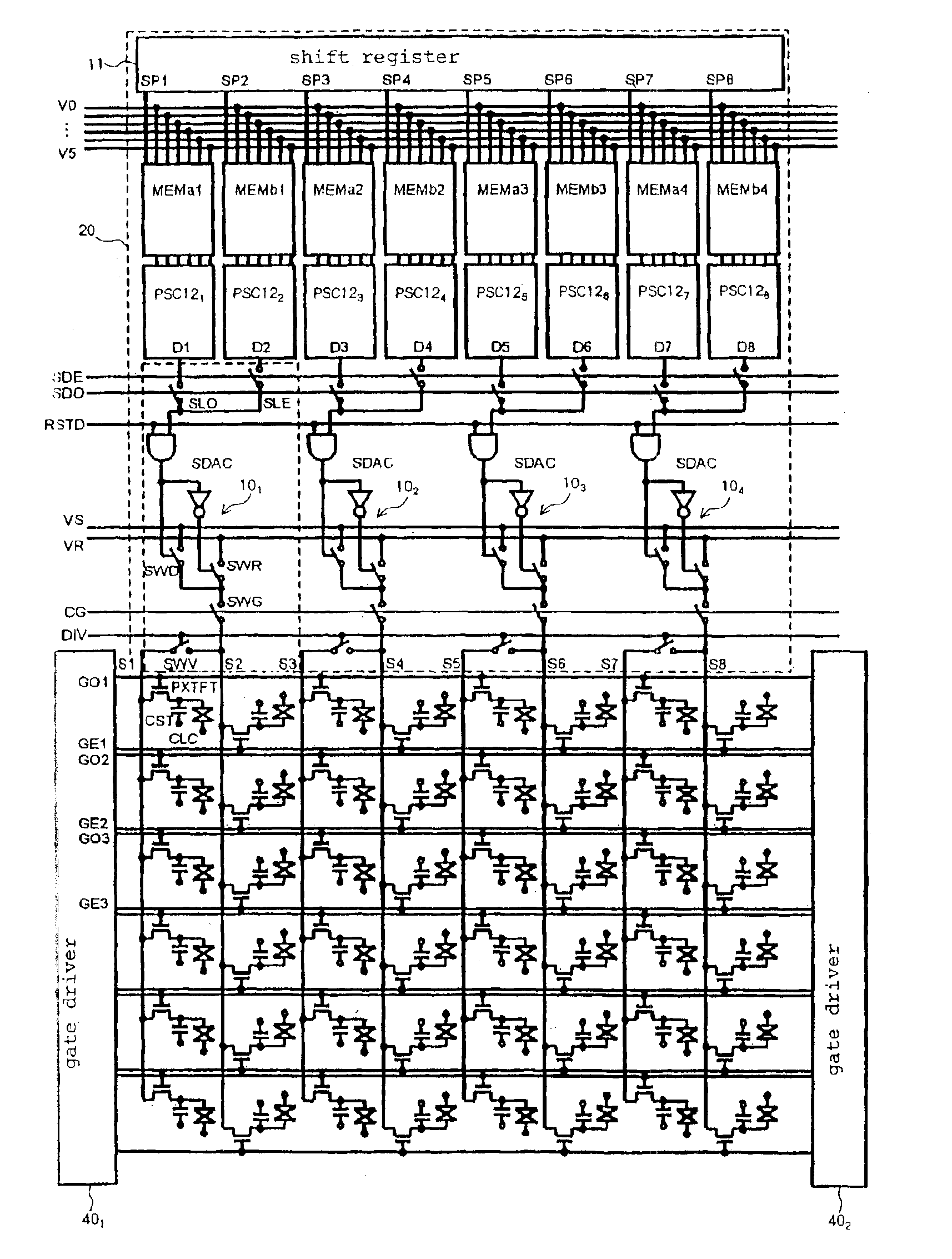
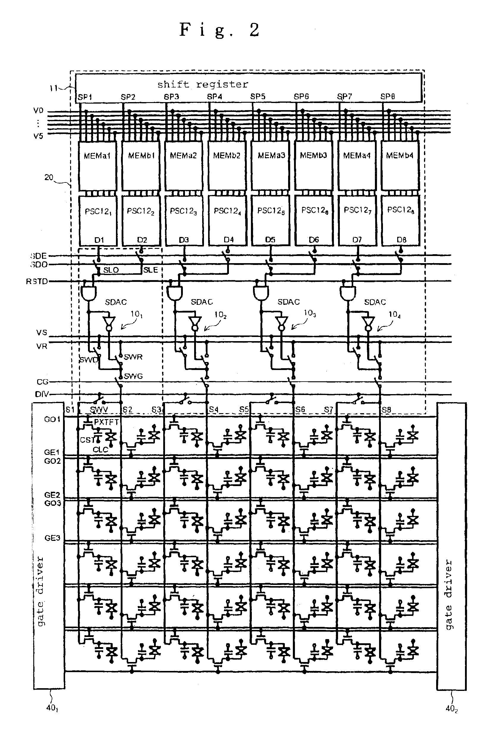
[0052]The construction of the liquid crystal display device that is the first embodiment of the display device of the present invention is next explained with reference to FIG. 2. For the purpose of explanation, the number of data bits of image signals V0-V5 is taken as six bits.

[0053]Referring now to FIG. 2, the liquid crystal display device of this embodiment consists of: pixel matrix in which a plurality of pixels are arranged in a matrix; data driver 20 for driving signal lines that are connected to the source terminals of the pixel TFTs of each pixel; and gate drivers 401 and 402 for driving the scanning lines that are connected to the gate terminals of the pixel TFTs. The pixel matrix consists of pixel TFTs, which are active elements for each pixel, and liquid crystal capacitance and storage capacitance that are connected to the drain terminals of the pixel TFTs. In the pixel matrix, moreover, one signal line is arranged for each pixel column, and two scanning lines are arrang...

second embodiment

[0089]Explanation next regards the liquid crystal display device that is the second embodiment of the present invention. We first refer to FIG. 20, which is a block diagram showing the construction of the liquid crystal display device of the second embodiment of the present invention. In FIG. 20, constituent elements that are identical to constituent elements in FIG. 2 are identified by the same reference numerals, and redundant explanation is omitted.

[0090]In the liquid crystal display device of the first embodiment that was previously described, all scanning lines are common to and driven by two gate drivers 401 and 402 that are arranged to the left and right of the pixel matrix; but as shown in FIG. 20, the two scanning lines GO and GE that are provided for each pixel row may each be independently driven by two gate drivers 411 and 412 that are provided to the left and right of the pixel matrix. In this case, the two gate drivers 411 and 412 can be realized by the circuits shown ...

third embodiment

[0093]An EL image display device, which is the display device of the third embodiment of the present invention, is next explained. FIG. 25 is a block diagram showing the construction of the EL display device of the third embodiment of the present invention. In FIG. 25, constituent elements that are identical to constituent elements in FIG. 1 are identified by the same reference numerals, and redundant explanation is here omitted.

[0094]In the liquid crystal display device of the first embodiment that was previously described, an example was described in which each of the pixels that make up the pixel matrix consists of a liquid crystal pixel. The EL display device that is the third embodiment, however, is an example of an EL image display device in which each pixel is made up by transistors, EL elements, and storage capacitance. FIG. 25 shows an example in which each of these pixels is made up by: two transistors, first transistor 70 and second transistor 71; EL element 60; and stora...


PUM


Abstract

A display device uses the load capacitances of two signal lines to perform DA conversion. Serial digital/analog conversion circuits (SDAC) in a data driver are provided for every two adjacent signal lines and use the load capacitances of these two signal lines to successively convert to analog data those data from the parallel/serial conversion circuits (PSC), PSC that correspond to the pixels of odd-numbered pixel columns and apply the converted analog data to the pixels of odd-numbered pixel columns, and successively apply data from PSC that correspond to the pixels of even-numbered pixel columns to the pixels of even-numbered pixel columns. Because the source of error of the SDAC is determined only by the difference between the two load capacitances, a polysilicon liquid crystal display device may be and the characteristics of the TFT may consequently show fluctuation, but will not act as an error source.

Description

BACKGROUND OF THE INVENTION[0001]1. Field of the Invention[0002]The present invention relates to display devices such as an organic EL (Electro Luminescence) image display device and a liquid crystal display device that are provided with a pixel matrix in which a plurality of pixels are arranged in matrix form, and more particularly to an organic EL image display device and liquid crystal display device for receiving digital image signals and driving each pixel of the pixel matrix, as well as to a method of driving such devices.[0003]2. Description of the Related Art[0004]Owing to their superior display characteristics, active matrix-type liquid crystal display devices in which TFT (Thin-Film Transistors), which are active elements, are provided in each pixel have become the mainstream in current liquid crystal display devices. Among these active matrix liquid crystal display devices, the current trend is towards devices that employ polysilicon TFTs as the active elements. This is b...

Claims


Application Information

Patent Timeline
IPC IPC(8): G02F1/13G02F1/133G09G3/36G09G3/20G09F9/30G09F9/35G09G3/30
CPCG09G3/3688G09G3/30G09G3/3655G09G2310/027G09G2310/0297
Inventor SEKINE, HIROYUKI
Owner VISTA PEAK VENTURES LLC
Why Eureka
Try Eureka