
All-optical XOR gate by using semiconductor optical amplifiers

a technology of optical amplifiers and logic gates, applied in logic circuits using specific components, pulse techniques, instruments, etc., can solve the problems of difficult application to optical calculation systems requiring high density integration, speed and capacity barriers in all silicon material and electric signals, and inability to meet large-scale fabrication requirements, etc., to achieve stable and easy combination, reduce the size and speed limitation of logic elements

Inactive Publication Date: 2005-08-16
KOREA INST OF SCI & TECH
View PDF2 Cites 7 Cited by
  • Summary
  • Abstract
  • Description
  • Claims
  • Application Information

AI Technical Summary

Benefits of technology

The present invention provides a method for implementing all-optical XOR logic elements using cross-gain modulation (XGM) of semiconductor optical amplifiers. This method is more stable and easier to combine with other elements than optical fiber-based elements, and can reduce the size and speed limitation of logic elements by eliminating the need of clock signal or CW light. The XOR logic elements can be realized without clock signal or CW light dependence, and various forms of logic can be realized using only one all-optical XOR logic element.

Problems solved by technology

However, almost all calculation systems based on silicon material and electric signals have barriers in speed and capacity.
Aforementioned elements using UNI, TOAD, and Sagnac gate have the advantage of high operation speed but are difficult to apply to optical calculation systems requiring high density integration because their core element is optical fiber that is difficult to integrate with other elements.
A forementioned IWC is an element made by integrating these semiconductor optical amplifiers, but not suitable for large-scale fabrication due to its complicated fabrication process.

Method used


Image

  • All-optical XOR gate by using semiconductor optical amplifiers
  • All-optical XOR gate by using semiconductor optical amplifiers
  • All-optical XOR gate by using semiconductor optical amplifiers

Examples


Embodiment Construction

[0023]Hereinafter, the constitution and operation of the present invention is described in detail through preferred embodiments by referring to the accompanying drawings.

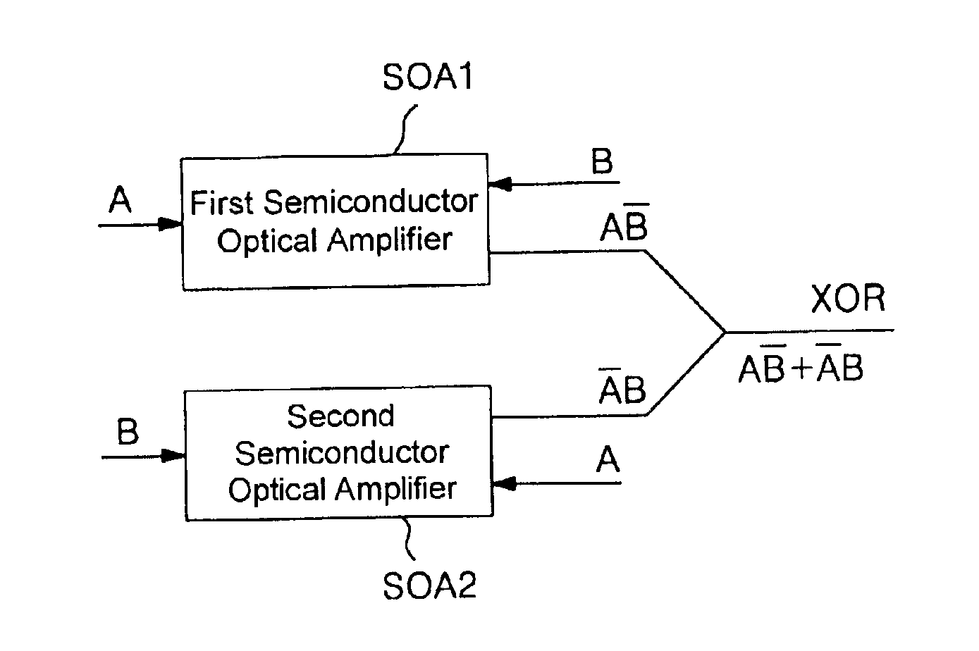
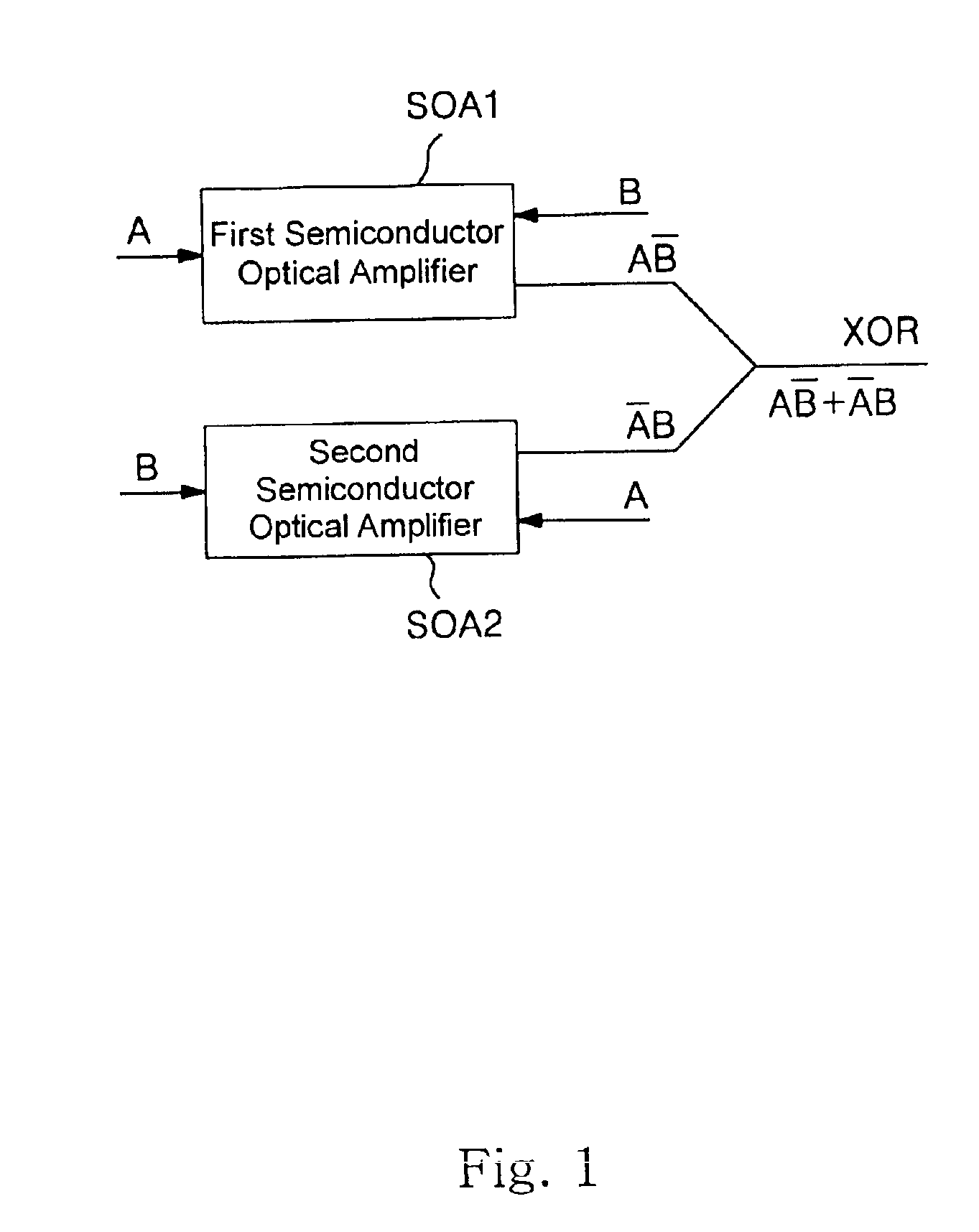
[0024]FIG. 1 shows the basic logic concept of XOR logic element in accordance with the present invention.

[0025]The XGM characteristic of semiconductor optical amplifiers (SOA1, SOA2) is adjustable by controlling input current, illumination signal, and pump-signal to the semiconductor optical amplifiers (SOA1, SOA2). The XGM characteristic is obtained by varying light intensity of pump-signal while maintaining increased state of input current at a fixed value and providing illumination signal at a constant light intensity.

[0026]Utilizing the above characteristic, in the first semiconductor optical amplifier (SOA1) signal A is modulated using signal B as pump-signal and signal A as illumination signal, while in the second semiconductor optical amplifier (SOA2) signal B is modulated using signal A as pump-signal and si...


PUM

PropertyMeasurementUnit
timeaaaaaaaaaa
speedaaaaaaaaaa
densityaaaaaaaaaa

Abstract

The present invention relates to a method of embodying all-optical XOR logic gate by using semiconductor optical amplifier, and more particularly, to a technique to embody all-optical XOR logic gate utilizing the cross-gain modulation (XGM) characteristic of semiconductor optical amplifiers controllable with input currents, illumination signal, and pumping signal.The method of all-optical XOR logic element in accordance with the present invention is characterized to obtain operational characteristic of the all-optical XOR logic element by inputting pump-signal and illumination signal concurrently into two semiconductor optical amplifiers and then summing the two output signals having XGM characteristic arising from gain saturation and wavelength conversion of the semiconductor optical amplifiers.

Description

BACKGROUND OF THE INVENTION[0001]1. Field of the Invention[0002]The present invention relates to a method of embodying all-optical XOR logic gate by using semiconductor optical amplifiers. More particularly, the present invention relates to a technique to embody all-optical XOR logic gate by utilizing the inverter characteristic of semiconductor optical amplifiers controllable with input currents, illumination signals, and pumping signals.[0003]2. Description of the Related Art[0004]In recent years, needs for high speed and large capacity of calculating systems have been increased. However, almost all calculation systems based on silicon material and electric signals have barriers in speed and capacity.[0005]On the other hand, calculation systems using optical elements based on InP are coping with such barriers of speed and information processing capacity.[0006]Generally, single optical logic elements such as AND, OR, XOR, NAND, NOR, and NXOR are integrated to constitute calculating...

Claims


Application Information

Patent Timeline
Patent Type & Authority Patents(United States)
IPC IPC(8): G02F3/00H01S3/10H01S5/50
CPCG02F3/00H03K19/14
Inventor KIM, JAE HUNBYUN, YOUNG TAEJHON, YOUNG MINLEE, SEOKWOO, DEOK HAKIM, SUN HOKANG, KWANG NAM
Owner KOREA INST OF SCI & TECH
Learn More