Memory device having different burst order addressing for read and write operations

a memory device and burst order technology, applied in the field of memory devices, can solve the problems of adding latency to the system, limiting the time required to transfer data between the processor and the computer,

Inactive Publication Date: 2005-08-16
ROUND ROCK RES LLC
View PDF9 Cites 6 Cited by
  • Summary
  • Abstract
  • Description
  • Claims
  • Application Information

AI Technical Summary

Problems solved by technology

A significant limitation on a computer's operating speed is the time required to transfer data between a processor and a memory circuit, such as a read or write data transfer.
However, be

Method used


Image

  • Memory device having different burst order addressing for read and write operations
  • Memory device having different burst order addressing for read and write operations
  • Memory device having different burst order addressing for read and write operations

Examples


Embodiment Construction

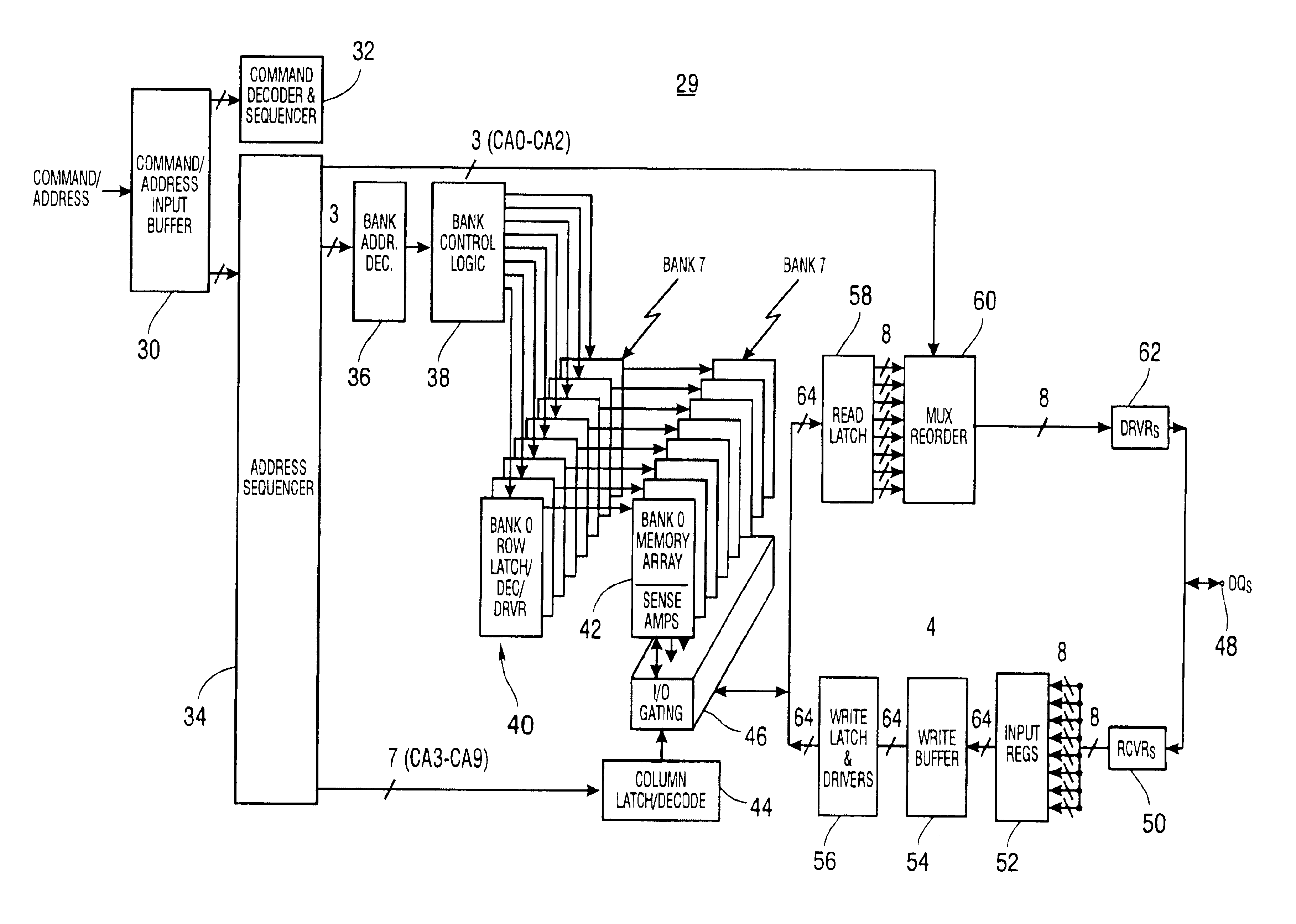
[0023]FIG. 3 illustrates a simplified block diagram of an architecture for a DRAM capable of implementing the burst read ordering of the present invention. The DRAM memory device 29 is comprised of a command / address input buffer 30 responsive to a command bus or command lines and an address bus or address lines. A command decoder and sequencer 32 and an address sequencer 34 are each responsive to the command / address input buffer 30.

[0024]A bank address decoder 36 is responsive to the address sequencer 34 while bank control logic 38 is responsive to the bank address decoder 36. A series of row latch / decoder / drivers 40 are responsive to the bank control logic 38 and the address sequencer 34. One row latch / decoder / driver 40 is provided for each memory array 42. Illustrated in FIG. 3 are eight memory arrays labeled bank 0 through bank 7. Accordingly, there are eight row latch / decoder / driver circuits 40 each responsive to one of bank 0 through bank 7.

[0025]A column latch / decode circuit 4...


PUM


Abstract

A method comprising reordering a block of n-bit words output from a memory array according to information in certain address bits before outputting at least one n-bit word from a memory device and ignoring said certain address bits before inputting at least one n-bit word into said memory array. The method may additionally comprise examining at least two of the least significant bits of a column address and wherein said reordering is responsive to said examining step. Thus, for reads a specific 8 bit burst is identified by the most significant column address bits while the least significant bits CA0-CA2 identify the most critical word and the read wrap sequence after the critical word. For writes, the burst is identified by the most significant column addresses with CA0-CA2 being “don't care” bits assumed to be 000.

Description

CROSS REFERENCE TO RELATED APPLICATIONS[0001]This application is a continuation of U.S. application Ser. No. 09 / 905,004 entitled “Memory Device Having Different Burst Order Addressing For Read and Write Operations”, filed 13 Jul. 2001 which issued on 17 Aug. 2004 as U.S. Pat. No. 6,779,074 B2, and is assigned to the same assignee as the present invention.BACKGROUND OF THE INVENTION[0002]1. Field of the Invention[0003]The present invention is directed to memory devices and, more particularly, to methods and circuits for reading information out of and writing information into the memory device.[0004]2. Description of the Background[0005]Computer designers are continually searching for faster memory devices that will permit the design of faster computers. A significant limitation on a computer's operating speed is the time required to transfer data between a processor and a memory circuit, such as a read or write data transfer. Memory devices such as dynamic random access memories (DRA...

Claims


Application Information

Patent Timeline
IPC IPC(8): G11C7/10G11C11/407G11C8/00G11C8/04G11C11/401
CPCG11C7/1018G11C7/1021G11C7/103G11C8/04G11C7/10
Inventor JANZEN, JEFFREY W.
Owner ROUND ROCK RES LLC
Why Eureka
Try Eureka