

Method of fabricating printed circuit board with mixed metallurgy pads
- Summary
- Abstract
- Description
- Claims
- Application Information
AI Technical Summary
Benefits of technology
Problems solved by technology
Method used
Image

Examples
Embodiment Construction
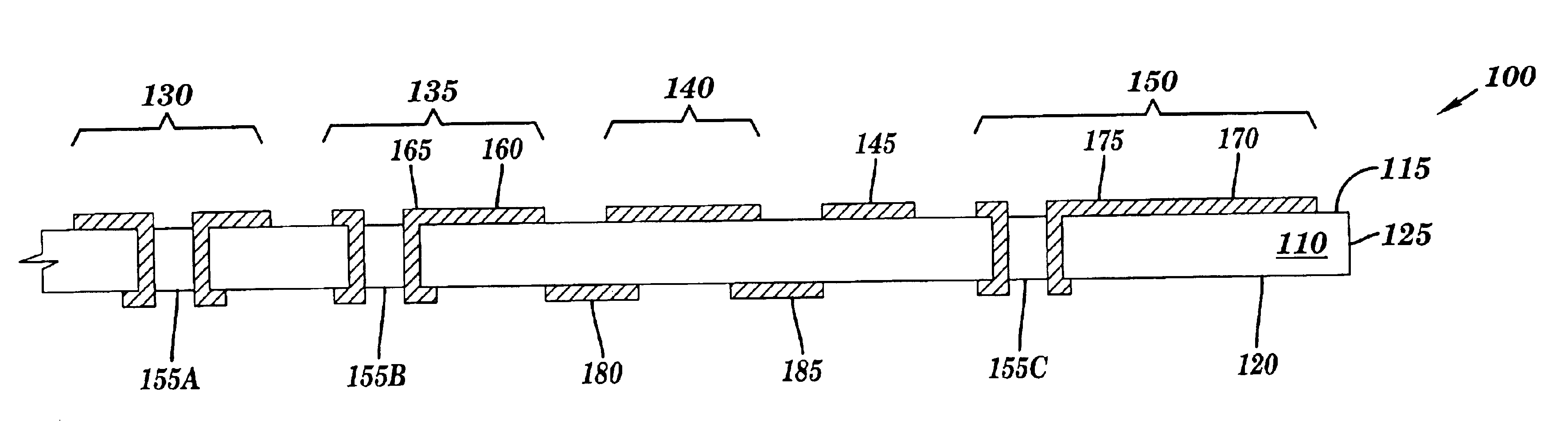
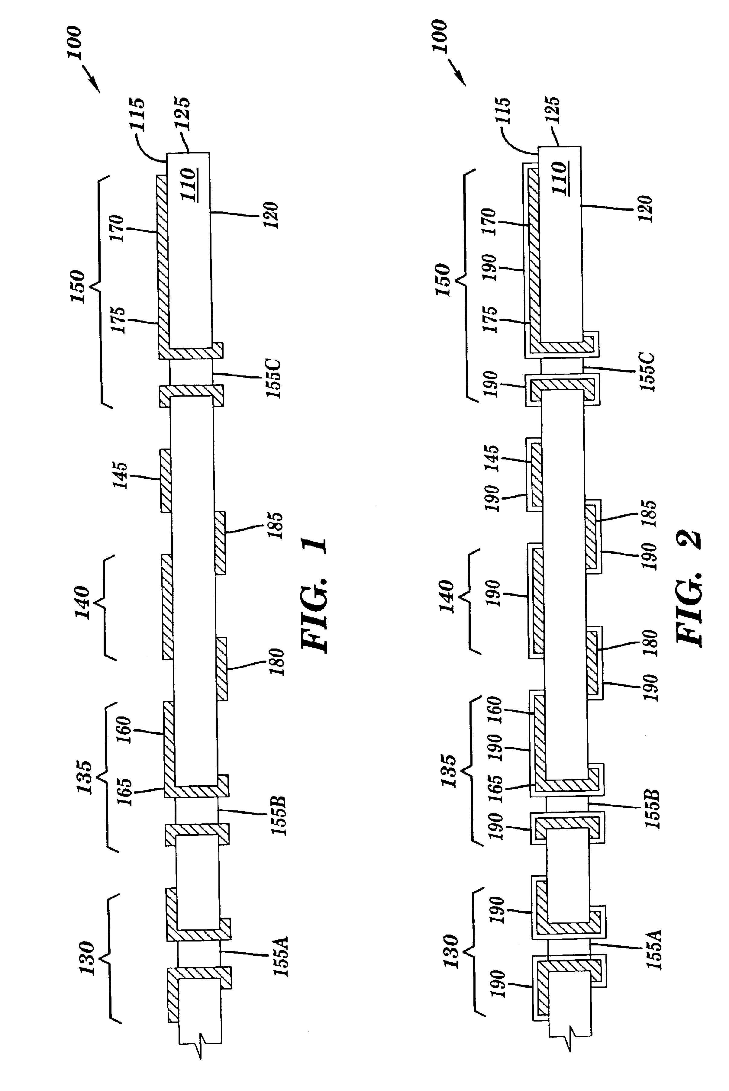
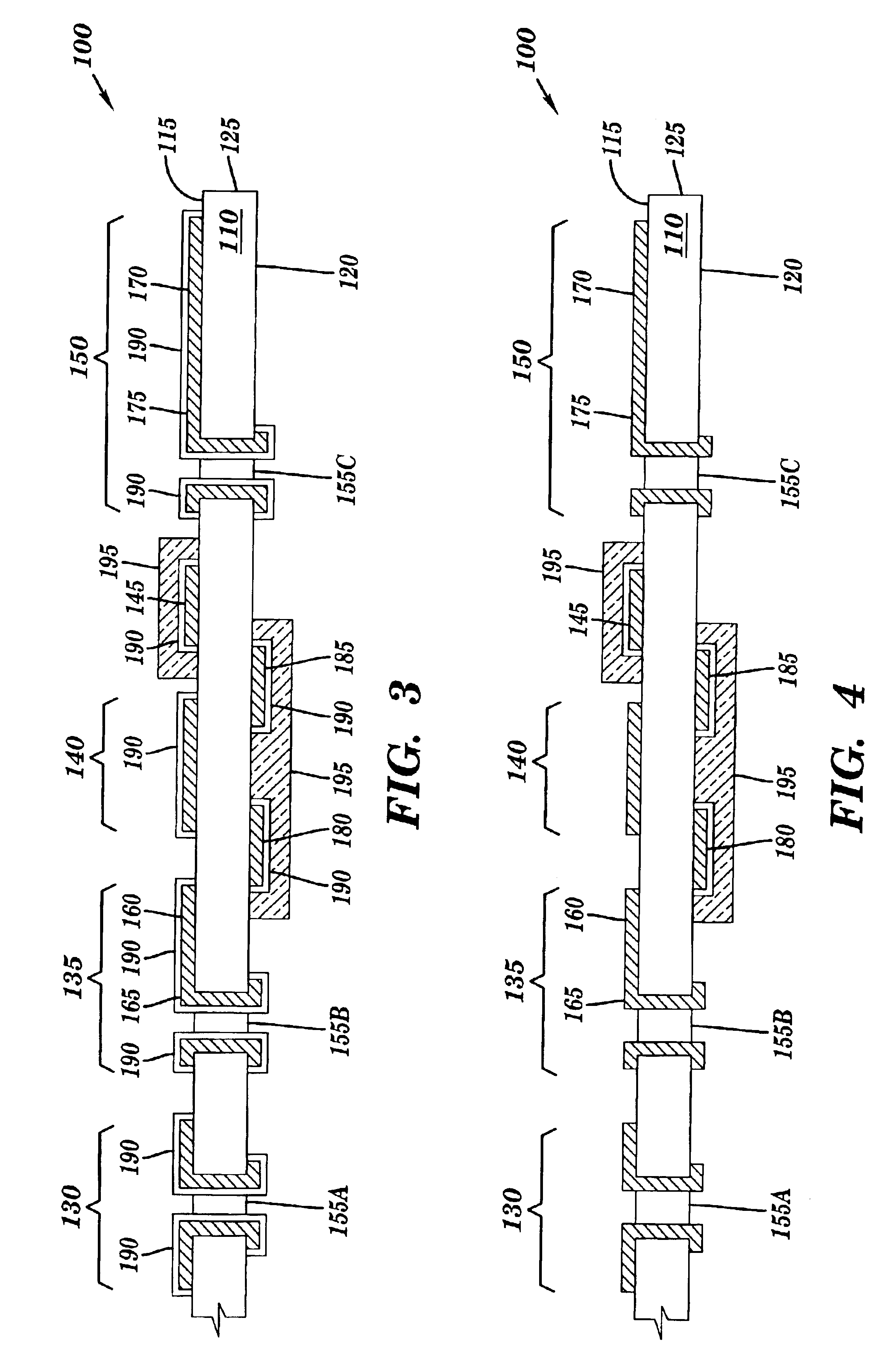
[0016]Referring to the drawings, FIGS. 1-6 show a sequence of partial cross section views illustrating initial process steps for fabricating a PCB according to the present invention. The process sequence starts with the structure illustrated in FIG. 1. In FIG. 1, PCB 100 includes a substrate 110 having a top surface 115, a bottom surface 120 and a substrate edge 125. In one example, substrate 110 is an insulating organic laminate board. In a second example, substrate 110 is a multi-layer organic laminate board having one or more internal wiring levels between layers of. laminate. In a third example, substrate 110 is a ceramic substrate. In a fourth example, substrate 110 is a multi-layer ceramic substrate having one or more internal wiring levels between layers of ceramic material. In a fifth example, substrate 110 is a flexible insulating polymer. Formed from copper on top surface 115 of substrate 110 is a PIH LGA pad 130, a LGA Pad 135, an SMT pad 140, a top wiring trace 145, and ...
PUM
| Property | Measurement | Unit |
|---|---|---|
| Thickness | aaaaa | aaaaa |
| Melting point | aaaaa | aaaaa |
Abstract
Description
Claims
Application Information