
Method of manufacturing semiconductor device using STI technique

a manufacturing method and semiconductor technology, applied in the field of semiconductor devices, can solve the problems of likely short circuit between floating gate electrodes

Inactive Publication Date: 2005-08-23
KK TOSHIBA
View PDF9 Cites 26 Cited by
  • Summary
  • Abstract
  • Description
  • Claims
  • Application Information

AI Technical Summary

Benefits of technology

[0008]The present invention has been achieved in view of the aforementioned problem, and therefore, an object of the present invention is to provide an STI technique wherein a gate insulation film and a gate electrode material film are successively formed at first and then, a device isolating film is buried, and which is improved so as to prevent the short circuit between the gate electrodes.
[0009]Another object of the present invention is to provide a semiconductor device and a manufacturing method of the semiconductor device, which are featured in that the occurrence of short circuit between gate electrodes can be substantially suppressed in the manufacturing process of semiconductor device.
[0013]As described above, according to the first and second aspects of the present invention, the gate electrode is formed so as to have a reverse tapered cross-section. If the gate electrode is formed into such a cross-sectional configuration, there would be little possibility that the patterning of the gate electrode is obstructed by the device isolating insulation film. Therefore, according to the first and second aspects of the present invention, it is possible to prevent the occurrence of short circuit between gate electrodes that might otherwise be induced by the etching residue.
[0022]In the method according to the second aspect of the present invention, the device isolating insulation film to be employed for filling the groove should preferably be formed in two steps as mentioned above. Namely, a first device isolating insulation film is formed inside the groove in a manner to make the groove into a forward tapered configuration in cross-section, and then, a second device isolating insulation film is formed inside the groove so as to fill the groove with the second device isolating insulation film. According to this method, the occurrence of short circuit between the gate electrodes due to an inappropriate filling of the groove can be prevented.

Problems solved by technology

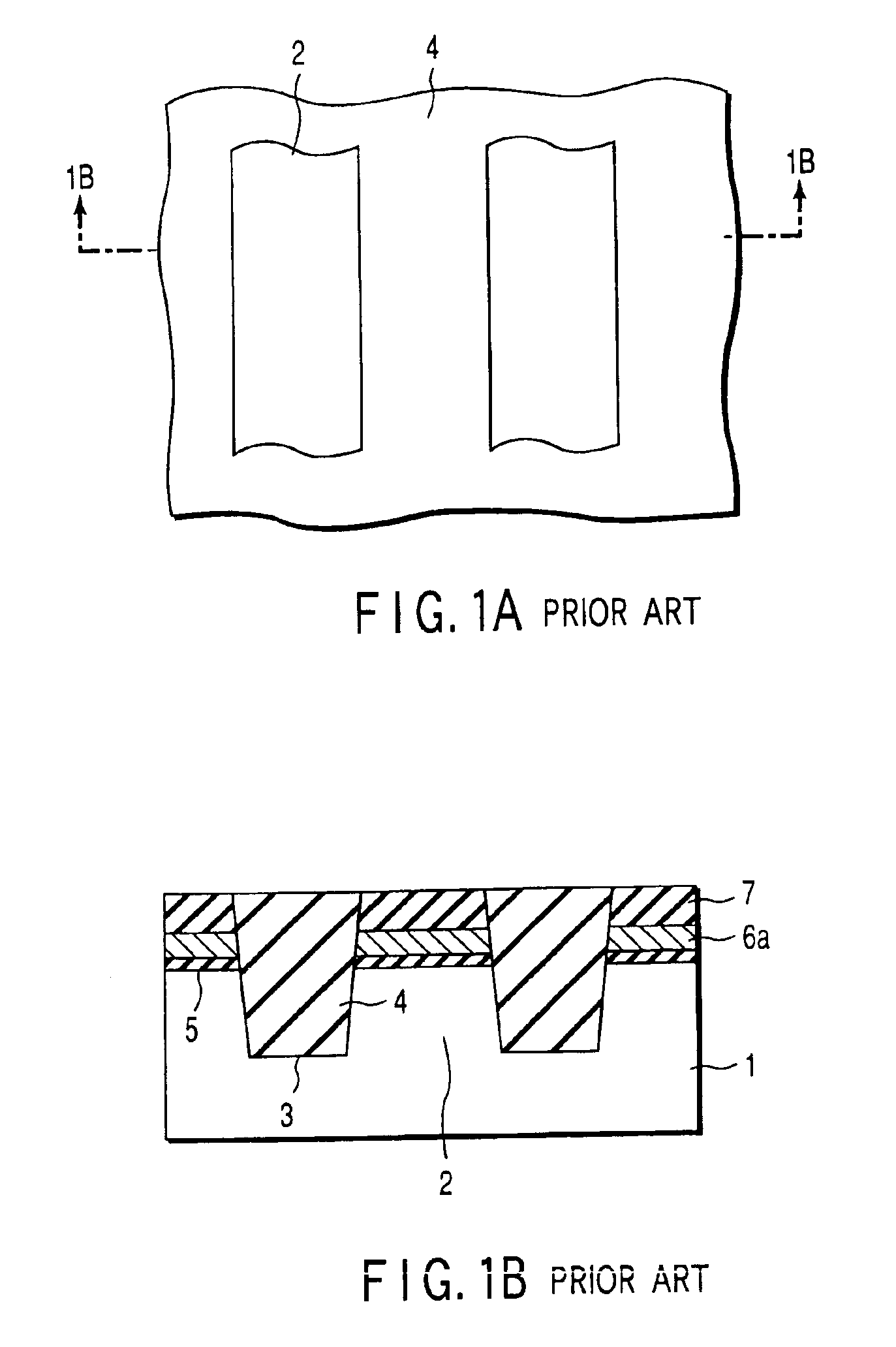
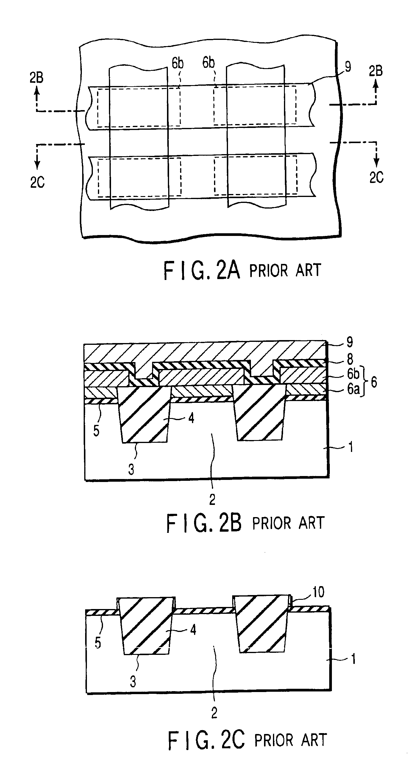
Namely, the conventional manufacturing process of the NAND type EEPROM where the aforementioned system [b] is utilized is accompanied with the problem that the short circuit between floating gate electrodes is likely to be occurred.

Method used


Image

  • Method of manufacturing semiconductor device using STI technique
  • Method of manufacturing semiconductor device using STI technique
  • Method of manufacturing semiconductor device using STI technique

Examples


first embodiment

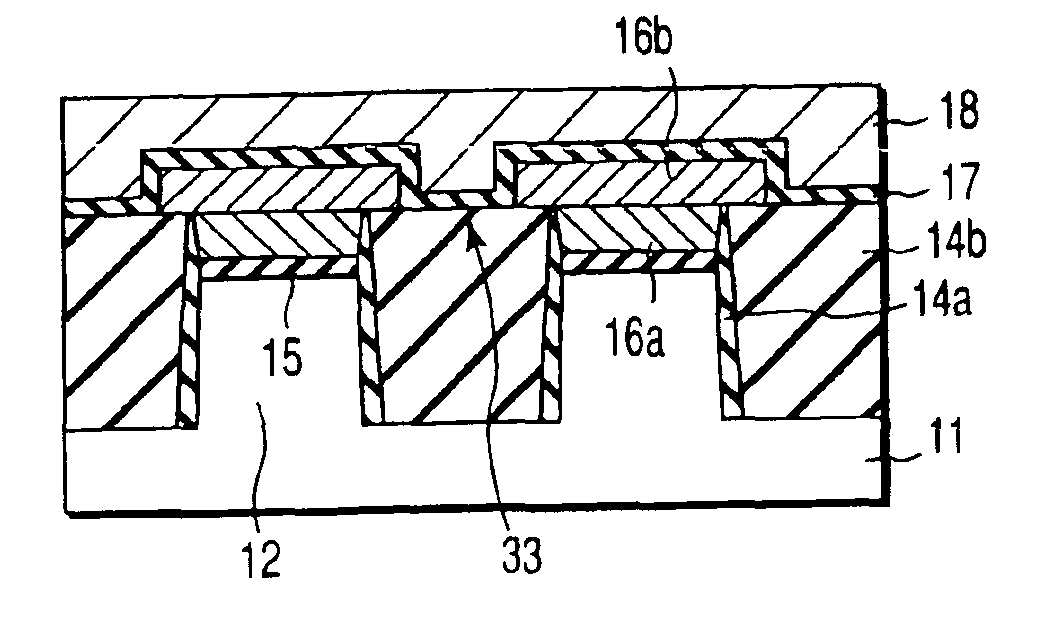
[0038]FIG. 3 is a plan view schematically showing the structure of the memory array portion of the NAND type EEPROM according to the present invention. FIG. 4A is a cross-sectional view taken along the line 4A-4A of the structure shown in FIG. 3, while FIG. 4B is a cross-sectional view taken along the line 4B—4B of the structure shown in FIG. 3.

[0039]Referring to the structure shown in FIGS. 3, 4A and 4B, a groove 13a for device isolating is formed by making use of an STI technique in one of the main surfaces of a p-type silicon substrate 11. This groove 13a is filled therein with a first device isolating insulation film 14a and a second device isolating insulation film 14b, both constituting a device isolating region. The element region 12 surrounded by these first device isolating insulation films 14a and second device isolating insulation films 14b is formed stripe-like, on which a gate insulation film (tunnel insulation film) 15 and a floating gate electrode 16 are successively ...

second embodiment

[0060]Next, the present invention will be explained. In this embodiment, the present invention is applied to the manufacture of a flash memory.

[0061]FIGS. 7A to 7H are views schematically showing the manufacturing process of the flash memory according to the second embodiment of the present invention; wherein FIGS. 7A, 7B, 7D and 7E are cross-sectional views each showing the manufacturing process; FIG. 7C is an enlarged partial cross-sectional view showing a portion of FIG. 7B; FIG. 7F is a plan view showing an accomplished structure; FIG. 7G is a cross-sectional view taken along the line 7G—7G of the structure shown in FIG. 7F; and FIG. 7H is a cross-sectional view taken along the line 7H—7H of the structure shown in FIG. 7F.

[0062]As shown in FIG. 7A, a silicon substrate 11 is heated in an oxygen gas atmosphere at a temperature of 800° C. to form a silicon oxide film 15 having a thickness of 10 nm on one of the main surfaces of the silicon substrate 11, the silicon oxide film 15 be...

third embodiment

[0075]Next, a third embodiment according to the present invention will be explained.

[0076]FIGS. 9A to 9C are cross-sectional views schematically illustrating the manufacturing process of the flash memory according to the third embodiment of the present invention. This third embodiment is almost the same as the second embodiment except that the method of forming the silicon oxide film 44a differs from that of the second embodiment.

[0077]Namely, first of all, in the same manner as explained in the second embodiment, a structure shown in FIG. 7A is obtained. Then, as shown in FIG. 9A, a silicon oxide film 44a having a film thickness of 20 nm is deposited on the surface of the structure by means of low pressure TEOS / O3 method at a temperature of 700° C. (alternatively, plasma CVD method at 400° C.). Then, as shown in FIG. 9B, the entire surface is subjected to RIE to remove the silicon oxide film 44a located outside the groove 43a, thus selectively leaving only the portion of the silico...


PUM


Abstract

A method of manufacturing a semiconductor device including forming a laminate structure which includes a gate insulation film on a semiconductor substrate and a gate electrode material film on the gate insulation film, processing the gate electrode material film to obtain a gate electrode having a reverse tapered cross section, and forming a device isolation insulation film in direct contact with a side surface of the gate electrode.

Description

CROSS-REFERENCE TO RELATED APPLIATIONS[0001]This is a divisional application of, and claims priority from, Application Ser. No. 09 / 892,487, filed Jun. 28, 2001 now U.S. Pat. No. 6,642,568. This application is based upon and claims the benefit of priority from the prior Japanese Patent Application No. 2000-197801, filed Jun. 30, 2000, the entire contents of which are incorporated herein by reference.BACKGROUND OF THE INVENTION[0002]The present invention relates to a semiconductor device and a manufacturing method thereof. In particular, the present invention relates to a semiconductor device to be produced through the utilization of STI technique which is designed such that a gate insulation film and a gate electrode are successively formed at first and then a device isolating insulation film is buried, and also to a manufacturing method which is applicable to the manufacture of such a semiconductor device.[0003]The STI (Shallow Trench Isolation) technique has been conventionally kno...

Claims


Application Information

Patent Timeline
IPC IPC(8): H01L21/70H01L21/762H01L27/115H01L21/8234H01L21/8247H01L21/28H01L21/76H01L29/423H01L29/43H01L29/49H01L29/788H01L29/792
CPCH01L21/76224H01L21/823481H01L27/115H01L27/11521H10B69/00H10B41/30H01L21/76
Inventor NARITA, KAZUHITOSAKAGAMI, EIJITSUNODA, HIROAKISONODA, MASAHISAKOBAYASHI, HIDEYUKI
Owner KK TOSHIBA
Learn More