Light-transmitting conductive material

a technology of conductive materials and conductive films, applied in the direction of dielectric characteristics, conductive layers on insulating supports, instruments, etc., can solve the problems of increasing electrical resistance, reducing total light transmittance, etc., and reducing pattern visibility and the occurrence of short circuits

Active Publication Date: 2019-10-15
MITSUBISHI PAPER MILLS LTD
View PDF28 Cites 0 Cited by
  • Summary
  • Abstract
  • Description
  • Claims
  • Application Information

AI Technical Summary

Benefits of technology

[0027]The present invention provides a highly sensitive optically transparent conductive material in which the pattern visibility and the occurrence of short circuit are reduced.

Problems solved by technology

Yet, ITO conductive films have a high refractive index and high surface reflectivity, so that optically transparent conductive materials including an ITO conductive film unfortunately have a reduced total light transmittance.
In addition, due to low flexibility, such ITO conductive films are prone to crack when bent, resulting in an increased electrical resistance.

Method used

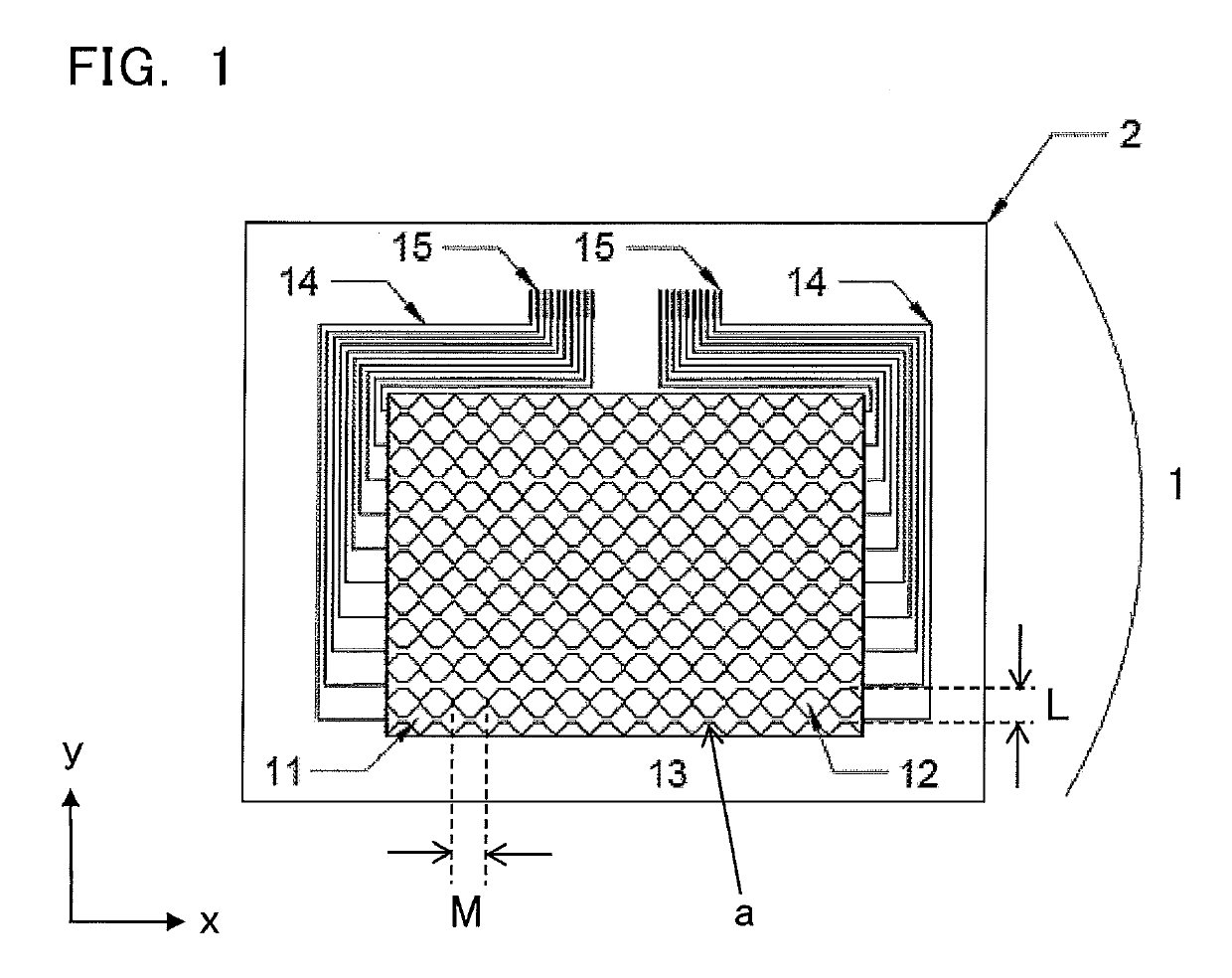
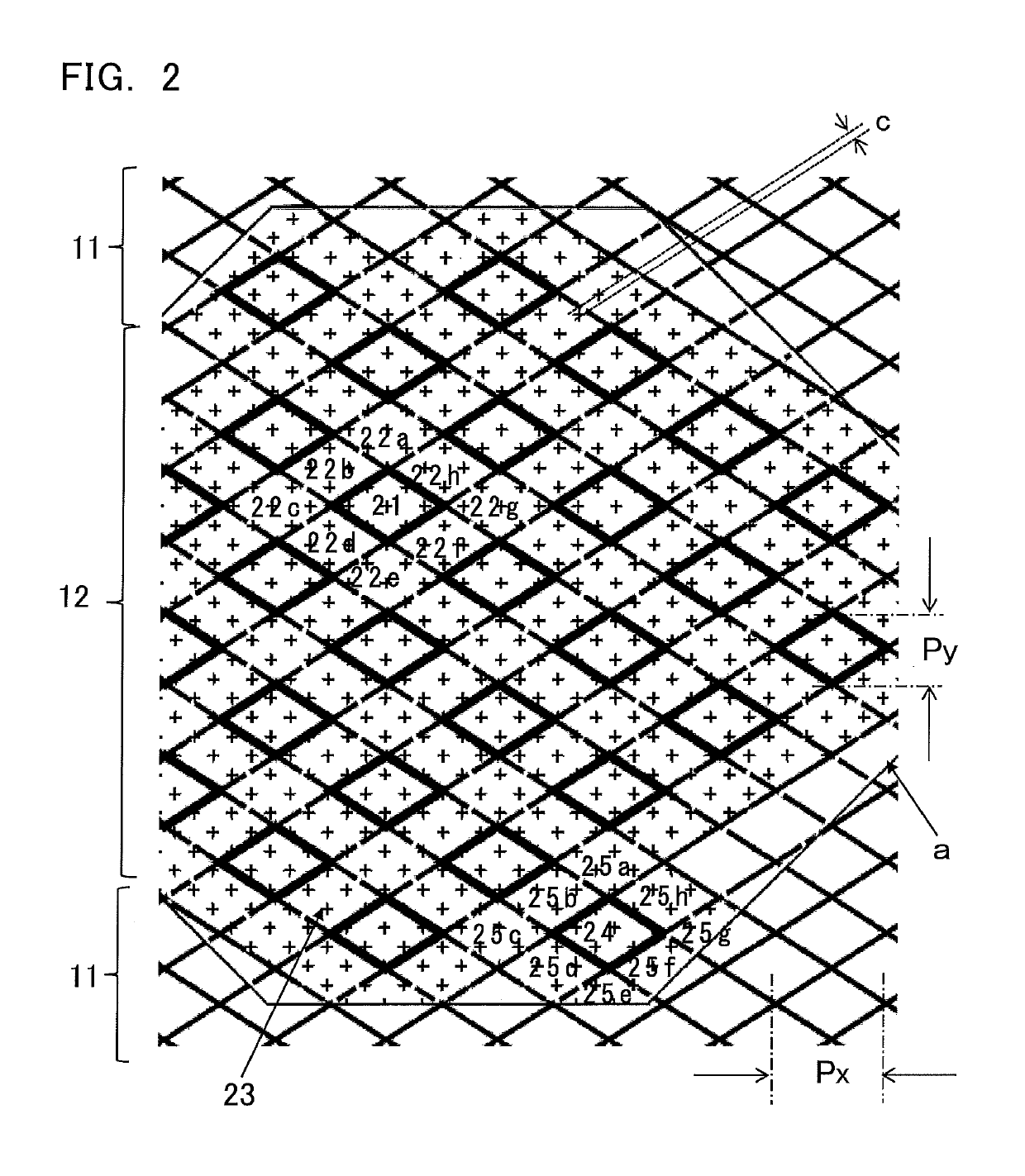
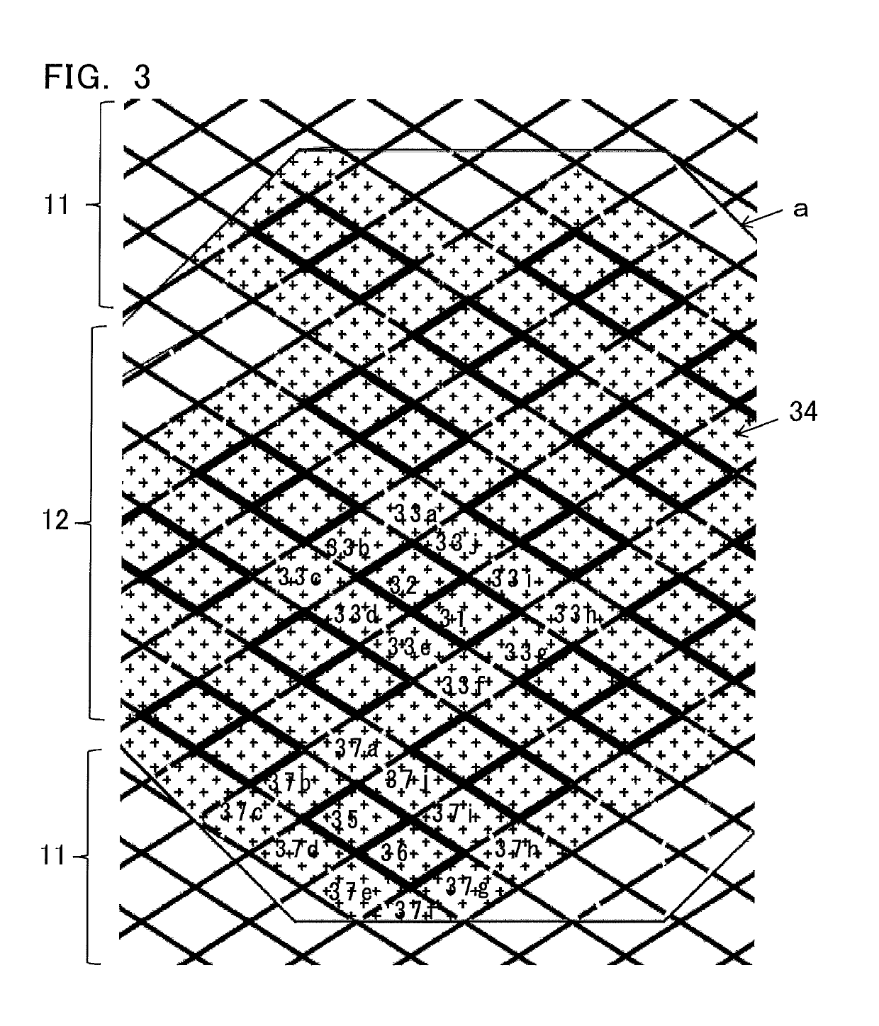

Image

  • Light-transmitting conductive material
  • Light-transmitting conductive material
  • Light-transmitting conductive material

Examples


examples

[0068]The present invention is described in detail below with reference to examples, but the present invention is not limited to the following embodiments within the scope of the invention.

1>

[0069]A 100-μm thick polyethylene terephthalate film was used as an optically transparent support. The total light transmittance of the optically transparent support was 91%.

[0070]Next, in accordance with the following formulation, the following physical development nuclei coating liquid was prepared, applied to the optically transparent support, and dried to form a physical development nuclei layer.

[0071]

Liquid A:Palladium chloride5gHydrochloric acid40mlDistilled water1000mlLiquid B:Sodium sulfide8.6gDistilled water1000ml

[0072]Liquid A and Liquid B were mixed with stirring for 30 minutes, and then passed through a column filled with an ion exchange resin to give a palladium sulfide sol.

for Each 1 m2

[0073]

Palladium sulfide sol prepared above0.4mg2% (by mass) aqueous solution of glyoxal0.2mlSur...


PUM

PropertyMeasurementUnit
widthaaaaaaaaaa
widthaaaaaaaaaa
widthaaaaaaaaaa

Abstract

An optically transparent conductive material including an optically transparent support, sensor parts electrically connected to a terminal area via peripheral wiring parts, and dummy parts not electrically connected to the terminal areas, the sensor parts and the dummy parts being disposed on the optically transparent support, wherein the sensor parts and the dummy parts each have a metal thin wire net-like pattern formed by an assembly of multiple polygons, the metal thin wire pattern of each dummy part includes disconnection parts, and the metal thin wire pattern of each dummy part also includes a region satisfying the following requirement (1) and / or a region satisfying the following requirement (2): (1) each polygon sharing one or more vertices with a polygon having no disconnection part includes at least one disconnection part; and (2) each polygon sharing one or more vertices with at least one of two polygons sharing a side or a vertex and having no disconnection part includes at least one disconnection part.

Description

TECHNICAL FIELD[0001]The present invention relates to an optically transparent conductive material for touchscreens, organic EL materials, solar cells, and the like. More specifically, the present invention relates to an optically transparent conductive material suitable for projected capacitive touchscreens.BACKGROUND ART[0002]Touchscreens are widely used as input means on displays of smart devices such as personal digital assistants (PDAs), laptop computers, smartphones, and tablet computers, as well as other electronic devices such as office automation equipment, medical equipment, and car navigation systems.[0003]There are various touchscreens that utilize different position detection methods, such as optical, ultrasonic, surface capacitive, projected capacitive, and resistive, touchscreens. Resistive touchscreens include an optically transparent conductive material and a glass plate with an optically transparent conductive layer, which face each other with a spacer therebetween...

Claims


Application Information

Patent Timeline
Patent Type & Authority Patents(United States)
IPC IPC(8): G06F3/041H01B5/14G06F3/044H05K1/02
CPCG06F2203/04103G06F2203/04112H05K2201/0108H05K1/0274G06F3/0443G06F3/0412H01B5/14
Inventor YOSHIKI, TAKENOBU
Owner MITSUBISHI PAPER MILLS LTD
Why Eureka
Try Eureka