Semiconductor structure and manufacturing method thereof

a technology of semiconductors and semiconductors, applied in the direction of semiconductor devices, electrical devices, transistors, etc., can solve the problems of short circuit between contacts and reduced active area, and achieve the effect of avoiding short circuit between contacts and reducing active area

a technology of semiconductors and semiconductors, applied in the direction of semiconductor devices, electrical devices, transistors, etc., can solve the problems of short circuit between contacts and reduced active area, and achieve the effect of avoiding short circuit between contacts and reducing active area

US20190006369A1Active Publication Date: 2019-01-03WINBOND ELECTRONICS CORP

Image

  • Semiconductor structure and manufacturing method thereof
  • Semiconductor structure and manufacturing method thereof
  • Semiconductor structure and manufacturing method thereof

Examples


Embodiment Construction

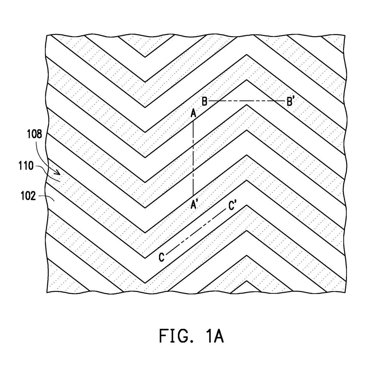
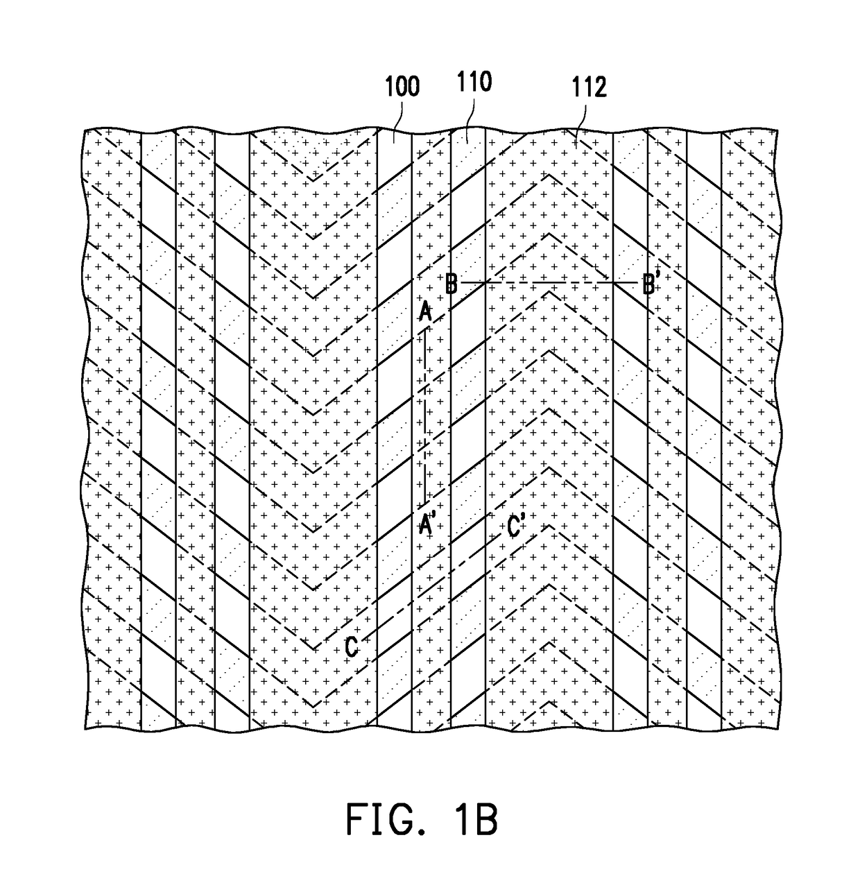
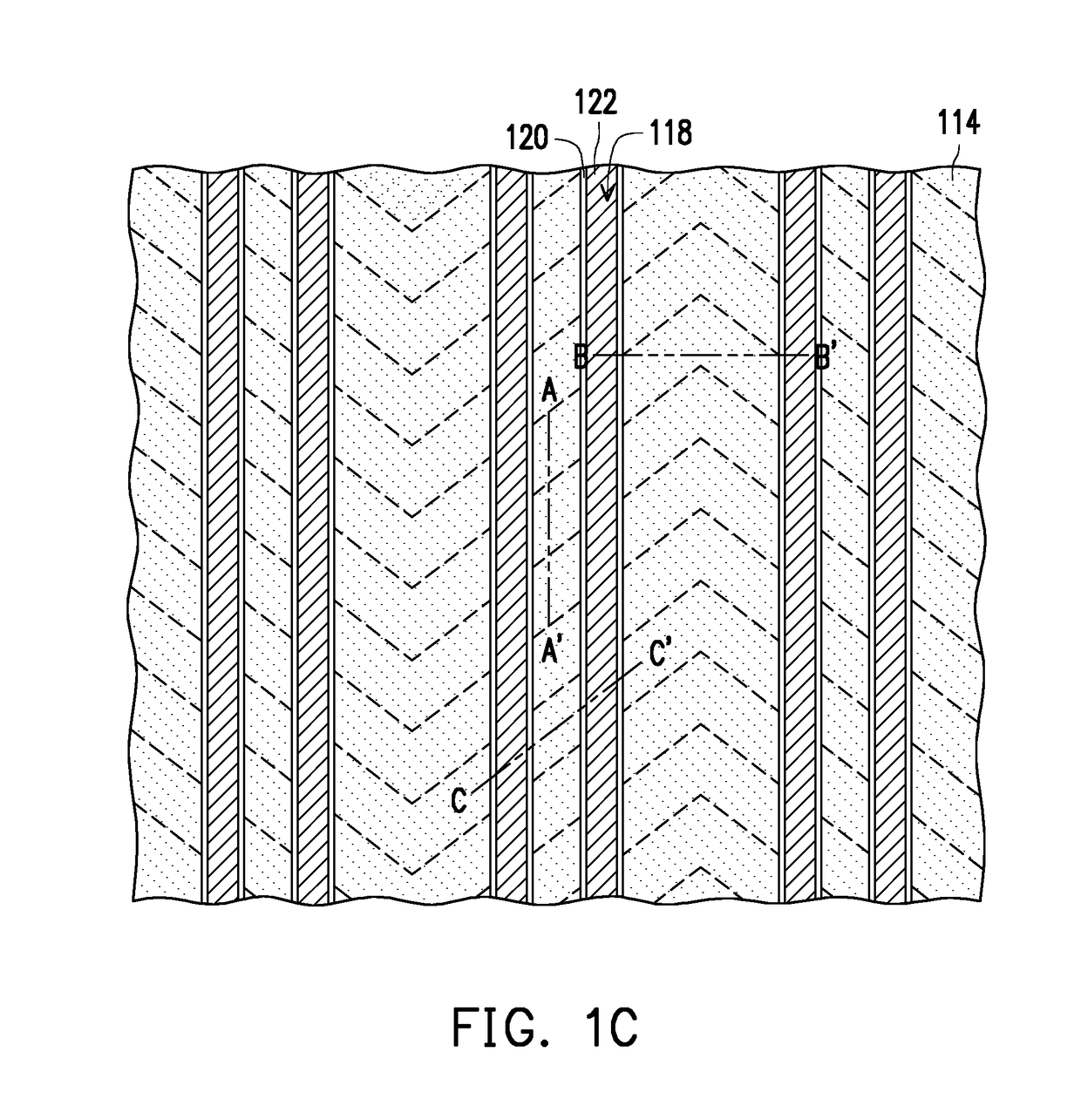
[0018]FIG. 1A to FIG. 1E are top views of a manufacturing process of a semiconductor structure according to an embodiment of the invention. FIG. 2A to FIG. 2E are cross-sectional views taken along section line A-A′ in FIG. 1A to FIG. 1E. FIG. 3A to FIG. 3E are cross-sectional views taken along section line B-B′ in FIG. 1A to FIG. 1E. FIG. 4A to FIG. 4E are cross-sectional views taken along section line C-C′ in FIG. 1A to FIG. 1E. The semiconductor structure of the invention may be implemented in a dynamic random access memory (DRAM).

[0019]Referring to FIG. 1A, FIG. 2A, FIG. 3A and FIG. 4A, a first patterned hard mask layer 102 is formed on a substrate 100. The substrate 100 may be a semiconductor substrate such as a silicon substrate.

[0020]The first patterned hard mask layer 102, for example, has a bent shape or a straight shape. In the present embodiment, the first patterned hard mask layer 102 has a bent shape. Such bent shape is conducive to an increase in contact area between an...


PUM


Abstract

A semiconductor structure includes a substrate, and first isolation structures, at least one buried word line and at least one second isolation structure which are disposed in the substrate. The buried word line intersects the first isolation structures. The second isolation structure intersects the first isolation structures. A material of at least a portion of the second isolation structure is different from a material of the first isolation structures.

Description

CROSS-REFERENCE TO RELATED APPLICATION[0001]This application claims the priority benefit of China application serial no. 201710532559.2, filed on Jul. 3, 2017. The entirety of the above-mentioned patent application is hereby incorporated by reference herein and made a part of this specification.BACKGROUNDTechnical Field[0002]The invention relates to a semiconductor structure and a manufacturing method thereof, and more particularly to a semiconductor structure including a buried word line and a manufacturing method thereof.Description of Related Art[0003]In a manufacturing process of a semiconductor device using a buried word line, intersecting isolation structures are formed in a substrate to define active areas. However, during subsequent formation of the buried word line, both a wet cleaning process and a thermal process may expand the isolation structures, leading to size reduction of the active area. Thus, contact area between a contact and the active area is accordingly reduce...

Claims


Application Information

Patent Timeline
03 Jan 2019
Publication
US20190006369A1
IPC
H01L27/108; H01L29/06; H01L21/762; H10B12/00
CPC
H01L27/10891; H01L27/10823; H01L27/10876; H01L29/0649; H01L21/76224; H01L21/762; H10B12/01; H10B12/00
Inventors
CHANG, WEI-CHE; TANAKA, YOSHINORI