Material for forming capacitor layer and method for manufacturing the material for forming capacitor layer

a technology of capacitor layer and manufacturing method, which is applied in the manufacture of fixed capacitors, fixed capacitor details, fixed capacitors, etc., can solve the problems of high long-term reliability, long time for dielectric breakdown, and thin film capacitors obtained by the method, so as to reduce the leakage current of the dielectric layer, reduce the leakage current, and reduce the effect of dielectric layer leakage curren

Inactive Publication Date: 2010-05-18
MITSUI MINING & SMELTING CO LTD
View PDF9 Cites 0 Cited by
  • Summary
  • Abstract
  • Description
  • Claims
  • Application Information

AI Technical Summary

Benefits of technology

[0035]The material for forming a capacitor layer according to the present invention achieves reduction of both occurrence of short circuit failures and a leakage current across a top electrode and a bottom electrode by impregnating a dielectric layer between a first conductive layer and a second conductive layer with a resin component. When the material for forming a capacitor layer is used as a capacitor, the material exhibits large capacitance and low dielectric loss. The dielectric layer performs its characteristics particularly when the dielectric layer is a dielectric oxide film formed by any one of a sol-gel method, an MOCVD method, and a sputtering deposition method. Furthermore, use of the method for manufacturing the material for forming a capacitor layer according to the present invention makes it possible to reduce a leakage current of a dielectric layer formed by the sol-gel method, the MOCVD method, or the sputtering deposition method and to efficiently manufacture materials for forming a capacitor layer having excellent dielectric characteristics.

Problems solved by technology

Patent Document 3 describes that thin film capacitors obtained by the method have higher long-term reliability and take a long time for dielectric breakdown.
However, the dielectric layers obtained by the sol-gel method, the MOCVD method or the sputtering deposition method have some problems, occurrence of a short circuit across a top electrode and a bottom electrode and occurrence of a large leakage current after formation of a capacitor due to its thin thickness of the layer because of uneven film thickness and gaps between oxide particles which result low production yields.
Particularly when the areas of electrodes are widened to increase the capacitance of a capacitor, defective products with short circuit may be frequently produced.

Method used


Image

  • Material for forming capacitor layer and method for manufacturing the material for forming capacitor layer
  • Material for forming capacitor layer and method for manufacturing the material for forming capacitor layer

Examples


example 1

(Manufacturing of Foil for Second Conductive Layer)

[0095]A 50-micron meter thick nickel foil manufactured by a rolling process was used herein. It should be noted that the thickness of the nickel foil manufactured by a rolling process is indicated as a thickness of a gauge.

(Manufacturing of Material for Forming Capacitor Layer)

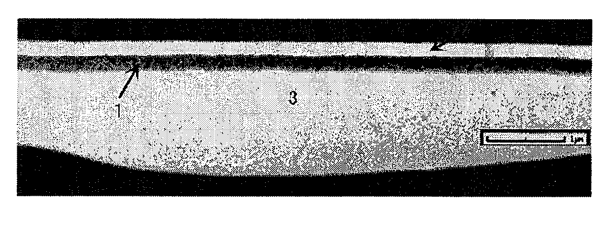
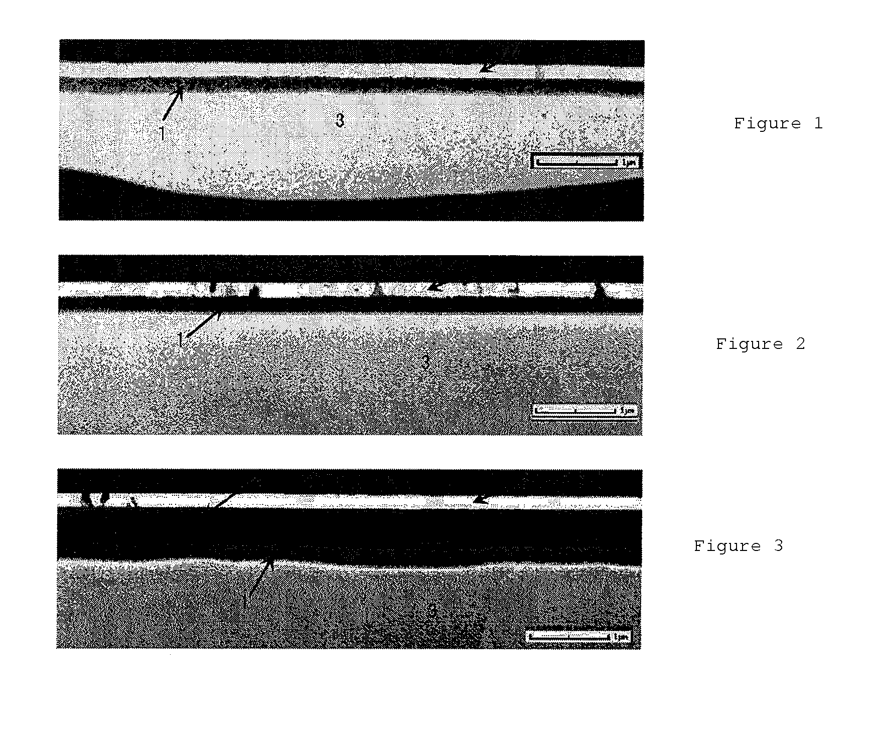
[0096]The nickel foil mentioned above was used for forming a second conductive layer to be used for forming a bottom electrode of a material for forming a capacitor layer. A dielectric layer was formed on the surface of the nickel foil by applying a sol-gel method. The nickel foil was subjected to a pretreatment before forming of the dielectric layer by the sol-gel method. The pretreatment was conducted by heating the nickel foil at 250° C. for 15 minutes and exposing the nickel foil to ultraviolet radiation for one minute.[0097](a) In this solution preparation process, a sol-gel solution to be used in the sol-gel method was prepared. This preparation was cond...

example 2

(Manufacturing of Foil for Second Conductive Layer)

[0111]A 50-micron meter thick nickel foil manufactured by a rolling process was used herein. It should be noted that the thickness of the nickel foil manufactured by a rolling process is indicated as a thickness of a gauge. The nickel foil would constitute the second conductive layer in a material for forming capacitor layer to be formed.

(Manufacturing of Material for Forming Capacitor Layer)

[0112]A dielectric layer was formed on the surface of the nickel foil by applying a sol-gel method. The nickel foil was subjected to a pretreatment before formation of the dielectric layer by the sol-gel method. The pretreatment was conducted by heating the nickel foil at 250° C. for 15 minutes and exposing the nickel foil to ultraviolet radiation for one minute.[0113]Process (a): In this solution preparation process, a sol-gel solution to be used in the sol-gel method was prepared. This preparation was conducted by using 7 wt % BST (trade name:...


PUM

PropertyMeasurementUnit
temperatureaaaaaaaaaa
thicknessaaaaaaaaaa
temperatureaaaaaaaaaa

Abstract

An object of the present invention is to provide a material for forming a capacitor layer comprising a dielectric layer formed by any one of a sol-gel method, an MOCVD method, and a sputtering deposition method. The material can reduce a leakage current of a capacitor circuit. In order to achieve the object, a material for forming a capacitor layer comprising a dielectric layer between a first conductive layer to be used for forming a top electrode and a second conductive layer to be used for forming a bottom electrode, characterized in that the dielectric layer is a dielectric oxide film formed by any one of a sol-gel method, an MOCVD method, and a sputtering deposition method; and particles constituting the dielectric oxide film are impregnated with a resin component is employed. In addition, a manufacturing method characterized in that the dielectric oxide film is formed on the surface of a material to be the bottom electrode by any one of a sol-gel method, an MOCVD method, and a sputtering deposition method; a resin varnish is impregnated into a surface of the dielectric oxide film; the resin is dried and cured to form the dielectric layer; and then a top electrode constituting layer is provided on the dielectric layer is employed.

Description

CROSS REFERENCE TO RELATED APPLICATION[0001]This application is a 35 U.S.C. 371 National Phase Entry Application from PCT / JP2006 / 308956, filed Apr. 28, 2006, which claims the benefit of Japanese Patent Application No. 2005-133693 filed on Apr. 28, 2005 in the Japanese Intellectual Property Office, the disclosure of which is incorporated herein in its entirety by reference.TECHNICAL FIELD[0002]The present invention relates to a material for forming a capacitor layer, a method for manufacturing the material for forming a capacitor layer, and a printed wiring board comprising an embedded capacitor layer obtained by using the material for forming a capacitor layer.BACKGROUND ART[0003]The material for forming a capacitor layer according to the present invention comprises a dielectric layer between a first conductive layer to be used for forming a top electrode and a second conductive layer to be used for forming a bottom electrode. Then the first conductive layer and the second conductiv...

Claims


Application Information

Patent Timeline
Patent Type & Authority Patents(United States)
IPC IPC(8): H01G4/22H01G4/005H01G4/20H01G4/33
CPCH01G4/1209H01G4/206H01G4/33H05K1/162Y10T428/265H05K2201/0175H05K2203/1147Y10T428/266H01G13/00
Inventor ABE, NAOHIKOSUGIOKA, AKIKOKANNO, AKIHIRONAKASHIMA, HIROTAKE
Owner MITSUI MINING & SMELTING CO LTD
Why Eureka
Try Eureka