

Thin-film photoelectric conversion device and method for production thereof
a conversion device and thin film technology, applied in the direction of solid-state devices, final product manufacturing, basic electric elements, etc., can solve the problems of reducing the power generation efficiency of the thin-film photoelectric conversion device, insufficient light absorption in the photoelectric conversion layer, and affecting the quality of the final product, so as to improve the fill factor and short circuit current and quantum efficiency
- Summary
- Abstract
- Description
- Claims
- Application Information
AI Technical Summary
Benefits of technology
Problems solved by technology
Method used
Image

Examples
example 1
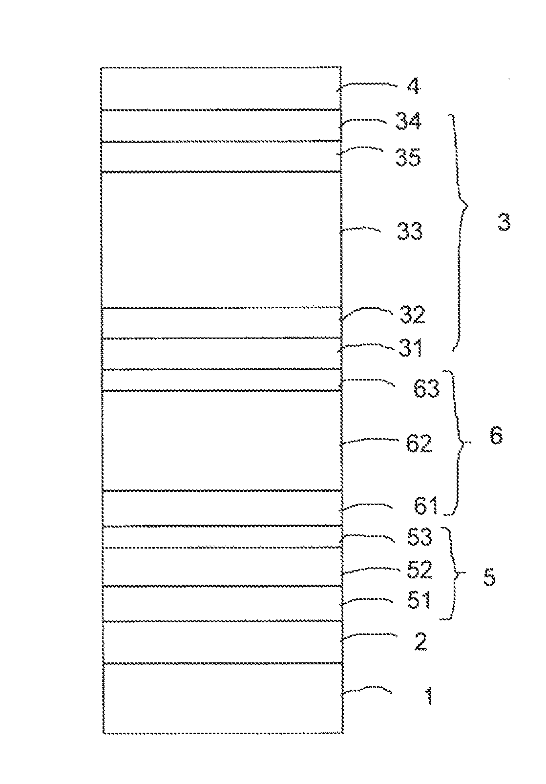
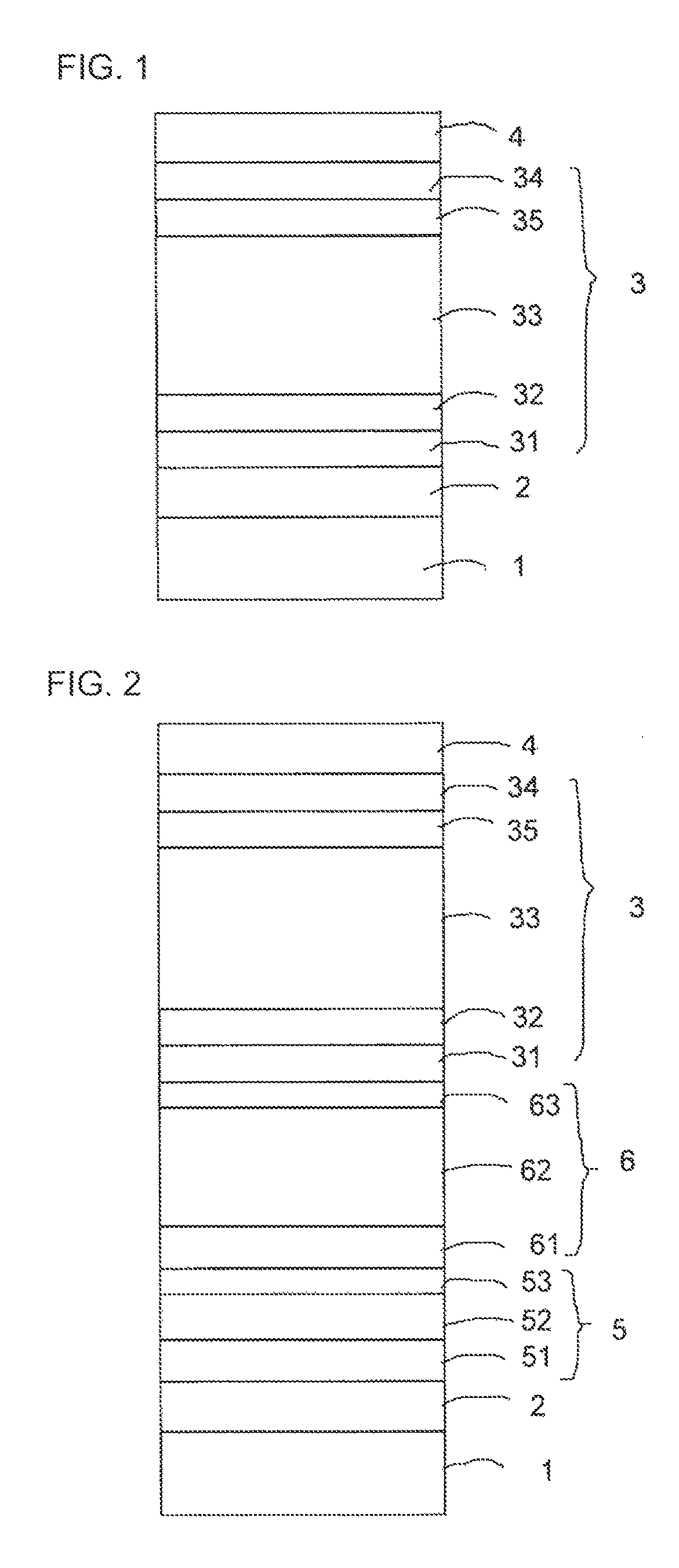
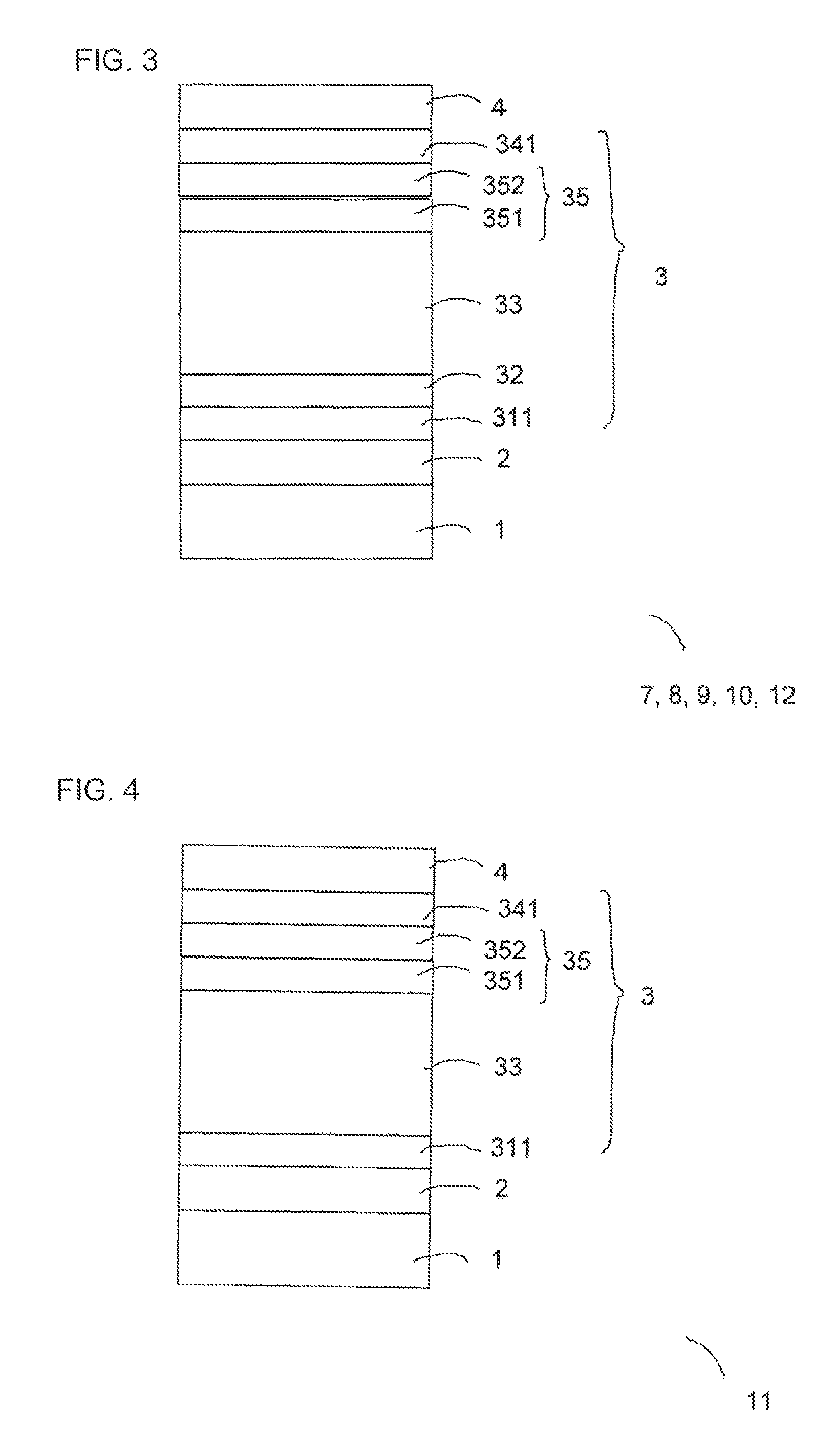
[0099]A single-junction thin-film photoelectric conversion device 7 having a structure shown in FIG. 3 was manufactured as Example 1. As a transparent substrate 1, a glass substrate having a thickness of 1.8 mm was used. As a transparent electrode 2, which is a first electrode layer, an SnO2 film having an average thickness of 700 nm, with fine pyramid-shaped surface irregularities contained therein was formed on the transparent substrate 1 by a thermal CVD method. Further, a ZnO film doped with Al was formed thereon with a thickness of 20 nm by using a sputtering method so that a transparent electrode layer 2 in which SnO2 and ZnO were stacked was formed. The resulting transparent electrode layer 2 had a sheet resistivity of about 9 Ω / sq. The haze ratio measured by using an illuminant C was 14%, and an average level difference d of the surface irregularities was about 100 nm.
[0100]The haze ratio was measured based upon JIS K7136.
[0101]On this transparent electrode layer 2, a crysta...
example 2
[0105]In Example 2, a single-junction thin-film photoelectric conversion device 8 similar to that of Example 1, which is shown in FIG. 3, was manufactured. The device in Example 2 was manufactured in the same manner as in Example 1, except the first interface layer 32, which is a substantially intrinsic amorphous silicon semiconductor layer, was formed to have a thickness of 5 nm.
example 3
[0106]In Example 3, a single-junction thin-film photoelectric conversion device 9 similar to that of Example 1, which is shown in FIG. 3, was manufactured. The device in Example 3 was manufactured in the same manner as in Example 1, except the first interface layer 32, which is a substantially intrinsic amorphous silicon semiconductor layer, was formed to have a thickness of 1 nm.
PUM
 Abstract
Description
Claims
Application Information