Interconnection structure and interconnection structure formation method

a technology of interconnection structure and interconnection structure, applied in the direction of semiconductor/solid-state device details, electrical devices, semiconductor devices, etc., can solve problems such as device signal delay, and achieve the effect of preventing a wiring delay and highly reliable interconnection structur

Inactive Publication Date: 2005-08-23
FUJITSU SEMICON LTD
View PDF9 Cites 21 Cited by
  • Summary
  • Abstract
  • Description
  • Claims
  • Application Information

AI Technical Summary

Benefits of technology

[0007]The present invention has been made to solve the above problem, and has as its object to provide an interconnection structure capable of preventing a wiring delay and obtaining a micropatterned, multilayer interconnection, and an interconnection structure formation method which realizes a highly reliable interconnection structure by solving various problems unique to the materials of the interconnection structure, e.g., elution of one material to the other.

Problems solved by technology

In a logic device having this multilayer interconnection, a wiring delay is becoming a dominant cause of a device signal delay.

Method used


Image

  • Interconnection structure and interconnection structure formation method
  • Interconnection structure and interconnection structure formation method
  • Interconnection structure and interconnection structure formation method

Examples


Embodiment Construction

Main Constitution of Present Invention

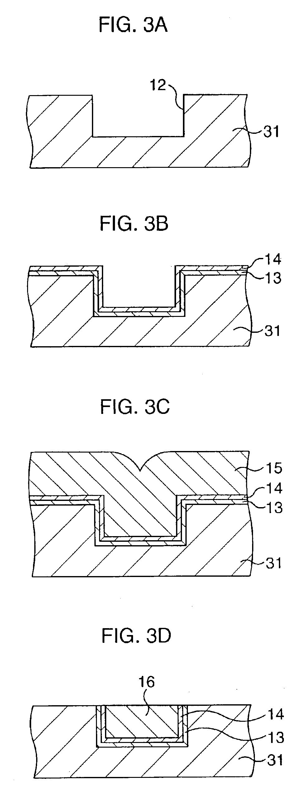
[0018]First, the main constitution of the present invention will be explained below along with its operating principle.

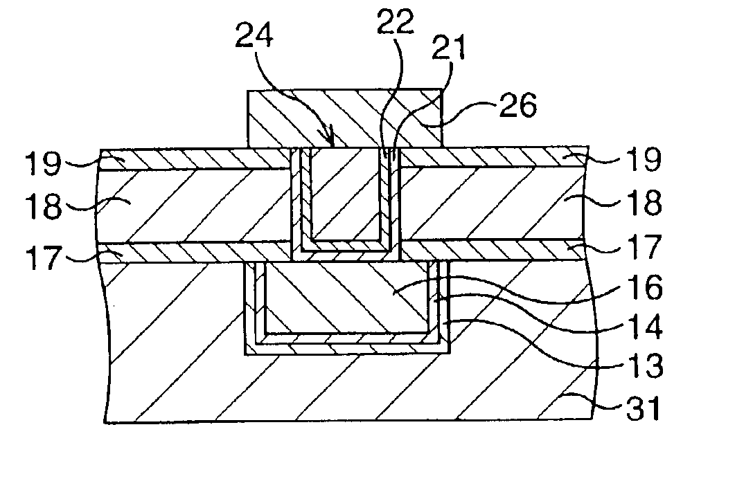
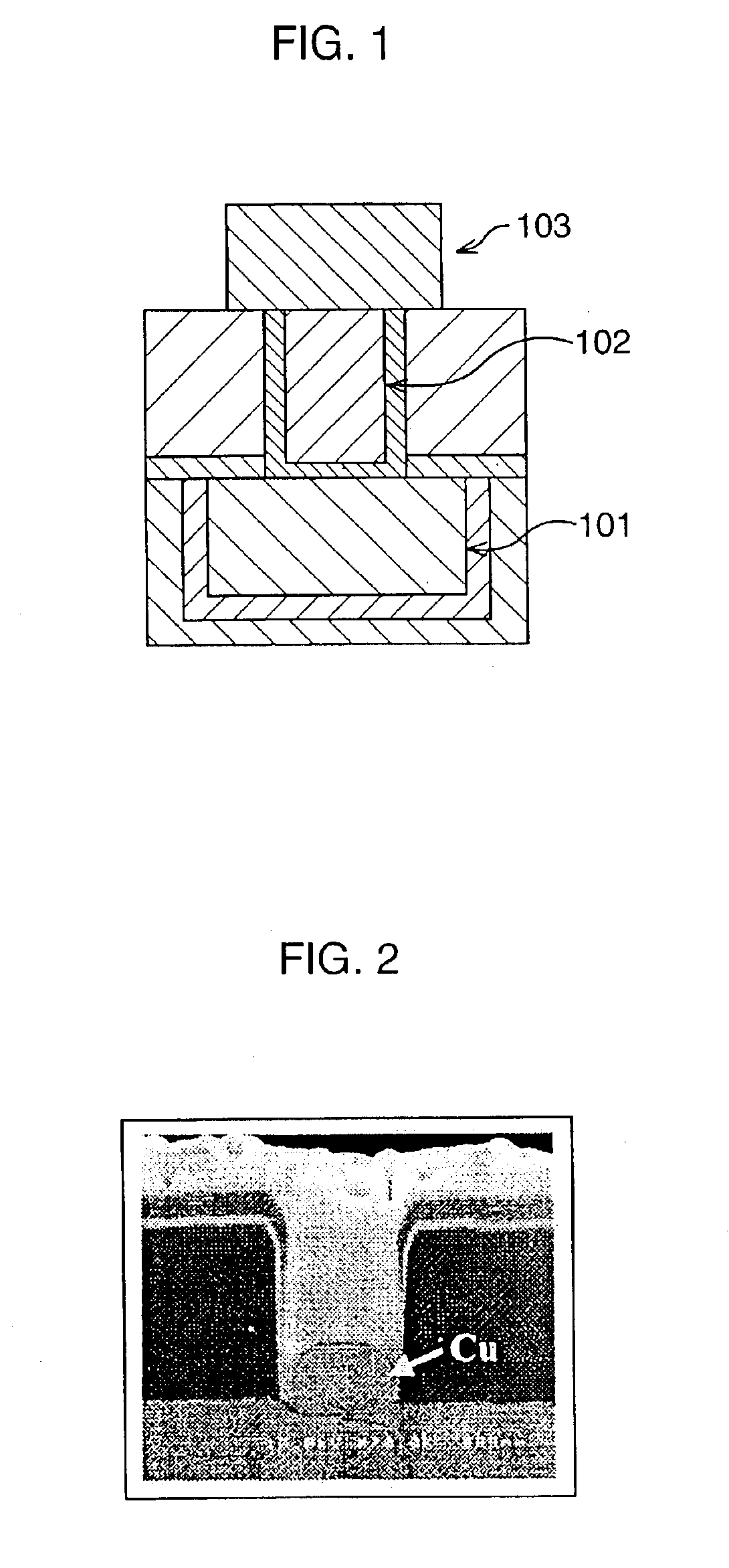
[0019]A representative example of a suitable metal material having low wiring resistance is copper (Cu). In the present invention, a Cu interconnection is used, and a refractory metal is used as a metal material for a contact of this Cu interconnection. The advantages of the use of a refractory metal as a burying material are that the interconnection reliability improves and the heat resistance does not easily fluctuate. A representative example of the refractory metal is tungsten (W).

[0020]When an interconnection structure using a Cu interconnection as the uppermost layer is formed, the moisture resistance may lower in a fuse formation process. Therefore, the present inventor studied how to improve the moisture resistance of the uppermost layer, and has found that an interconnection structure using a Cu interconnection as a low...


PUM


Abstract

An insulating film covering a Cu interconnection is formed. A contact hole which partially exposes the surface of the Cu interconnection is formed in the insulating film. A series of steps (steps (a) to (d)) including (a) a step of continuously supplying WF6 gas for a predetermined time, (b) a step of continuously exhausting the WF6 gas atmosphere for a predetermined time, (c) a step of continuously supplying SiH4 gas for a predetermined time, and (d) a step of continuously exhausting the SiH4 gas atmosphere for a predetermined time, is repeatedly executed to form W nuclei in the contact hole. Then, a W film is buried into the contact hole. This interconnection structure formation method can reliably bury the W film into the contact hole while preventing Cu elution from the Cu interconnection to the W plug.

Description

CROSS-REFERENCE TO RELATED APPLICATIONS[0001]This application is based upon and claims priority of Japanese Patent Application No. 2002-037393, filed on Feb. 14, 2002, the contents being incorporated herein by reference.BACKGROUND OF THE INVENTION[0002]1. Field of the Invention[0003]The present invention relates to an interconnection structure suitably applicable to a semiconductor device and a method of forming the same.[0004]2. Description of the Related Art[0005]As a conventional interconnection formation technique for semiconductor integrated circuits, a technique of forming a metal film represented by an aluminum (Al) film or an Al alloy film by sputtering is generally extensively used.[0006]However, to meet the recent demands for further downsized and integrated semiconductor devices, micropatterned interconnections and multilayer interconnections are acceleratedly advanced. In a logic device having this multilayer interconnection, a wiring delay is becoming a dominant cause o...

Claims


Application Information

Patent Timeline
Patent Type & Authority Patents(United States)
IPC IPC(8): H01L21/285H01L21/70H01L21/02H01L21/768
CPCH01L21/28562H01L21/76877
Inventor NARUKAWA, KUNIYUKI
Owner FUJITSU SEMICON LTD
Why Eureka
Try Eureka