Two-dimensional laser diode array light-emitting device

a technology of laser diodes and light-emitting devices, which is applied in the direction of semiconductor laser arrangements, lasers, and lasers. it can solve the problems of increasing the cost of assembling cooling assemblies to form a surface light-emitting device, the cost of bonding parts and assembly costs, and the heat generated by the laser diodes in the ld bar. it can reduce manufacturing costs and simplify the electrical connection structure. , the effect of reducing the manufacturing cos

Inactive Publication Date: 2005-08-23
FANUC LTD
View PDF2 Cites 67 Cited by
  • Summary
  • Abstract
  • Description
  • Claims
  • Application Information

AI Technical Summary

Benefits of technology

[0019]An object to the present invention is to provide a two-dimensional LD array light-emitting device constitute

Problems solved by technology

The laser diodes in the LD bar generate considerable heat when driven to raise temperature of the LD bar.
Particularly in a case of arranging adjacent LD bars close to each other so as to reduce a dead space (non-emitting region) between light-emitting regions of the LD bars in the surface light-emitting device, there arises a significant problem of how to effectively remove the heat generated by the LD bars.
The cost of the parts such as bonding parts and assemble cost, and cost for assembling the cooling assemblies to be stacked to form a surface light-emitting device are relatively increased by a ratio thereof in the whole manufacturing cost of the surface light-emitting device.
Reviewing the conventional structure in the above view,

Method used


Image

  • Two-dimensional laser diode array light-emitting device
  • Two-dimensional laser diode array light-emitting device
  • Two-dimensional laser diode array light-emitting device

Examples


first embodiment

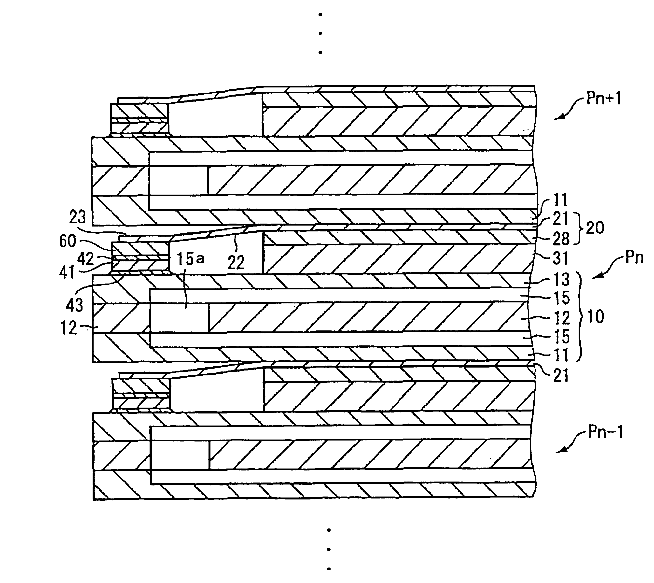
[0032]FIG. 1 shows a cross-sectional structure of a two-dimensional LD array surface light-emitting device according to the present invention. The light-emitting device comprises a large number of light-emitting units stacked successively. In FIG. 1, only three adjacent light-emitting units, an (n−1)th light-emitting unit Pn−1, an n-th light-emitting unit Pn and an (n+1)th light-emitting unit Pn+1 (n: integer not less than two) are depicted in light-emitting units P1-PN of the total number N which constitutes the surface light-emitting device.

[0033]An arrangement and a function of the n-th light-emitting unit Pn will be described as a representative of the plurality of light-emitting units P1-PN. The light-emitting unit Pn comprises a LD bar 60 and a cooling assembly 10 for cooling the LD bar 60 mounted thereon. A cooling assembly having a conventional structure may be adopted as the cooling assembly 10 as shown in an exploded view of FIG. 4. Particularly, the cooling assembly 10 ha...

second embodiment

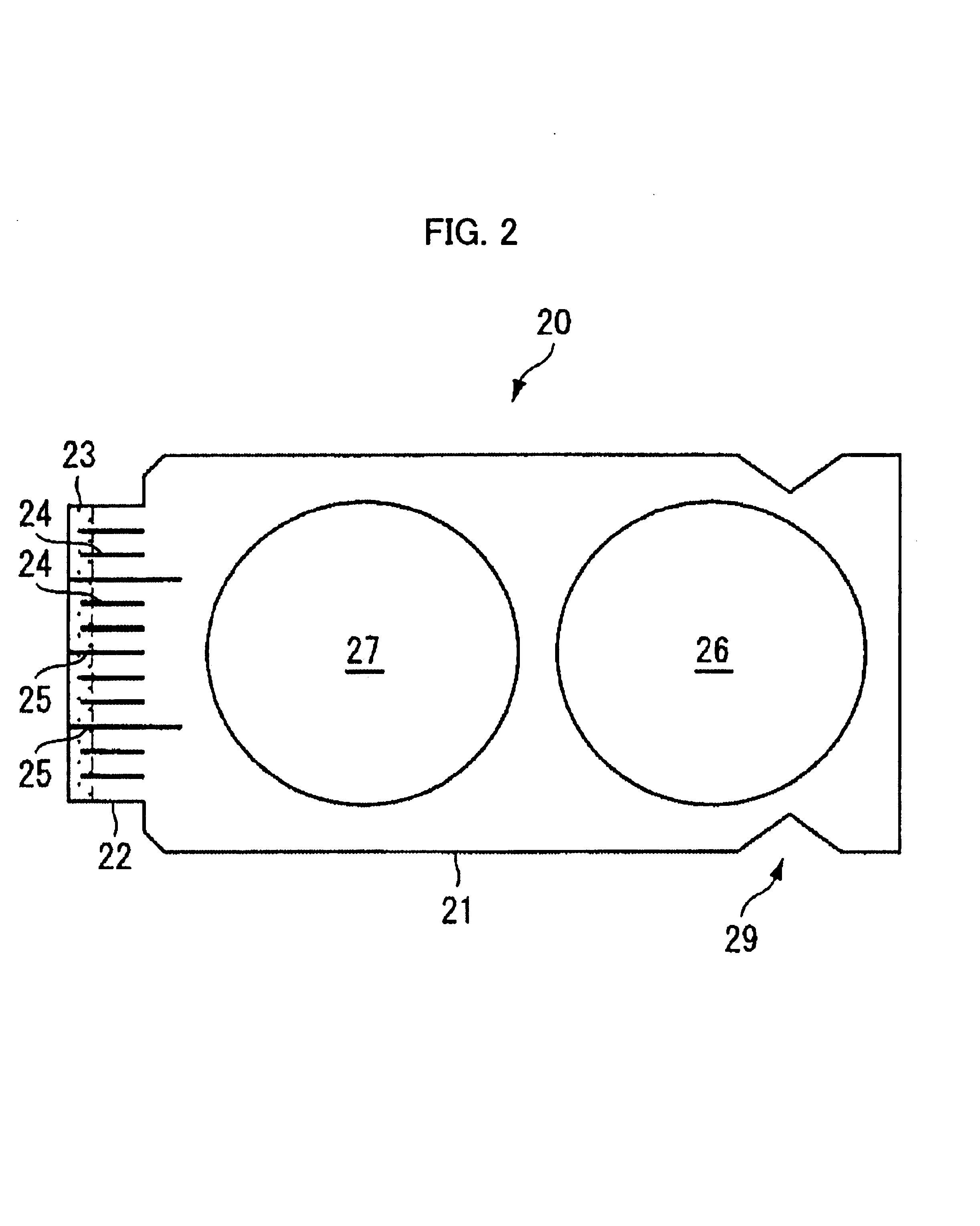
[0059]In this second embodiment, a spacer plate 32 is intervened between the copper layer of the TAB sheet 20 and the metal plate 11 of the cooling assembly 10 of the adjacent cooling assembly Qn+1. The spacer plate 32 is arranged for adjusting a distance between the cooling assembly 10 of the light-emitting unit Qn and the cooling assembly 10 of the adjacent light-emitting unit Qn+1 so that the connecting portion 23 of the TAB sheet 20 is not in contact with the cooling assembly 10 of the adjacent light-emitting unit Qn+1 when the light-emitting units P1-PN are stacked. The spacer plate 32 may be omitted if it is not necessary to adjust the distance between the cooling assemblies 10.

[0060]In this embodiment, the polyimide resin layer 28 of the TAB sheet 20 is confronting and in contact with the cooling assembly 10 of the light-emitting unit Qn without any member intervened therebetween in both cases of using and not using the spacer plate 32. The copper plate 21 of the TAB sheet 20...


PUM


Abstract

A two-dimensional LD (laser diode) array light-emitting device constituted by stacking light-emitting units each having a LD bar and a cooling assembly for cooling the LD bar with a simplified electrical connection structure to reduce manufacturing cost. The cooling assembly is electrically connected with one electrode of the LD bar through the die spacer so that a part of the cooling assembly serves as one electrode of the light-emitting unit. The other electrode of the LD bar is electrically connected with a webbed extending section of a conductive layer of a TAB (tape-automated bonding) sheet so that the conductive layer serves as the other electrode of the light-emitting unit. A space between the adjacent cooling assemblies for arranging the LD bar is adjusted by the spacer sheet intervened between the TAB sheet and the cooling assembly.

Description

BACKGROUND OF THE INVENTION[0001]1. Field of the Invention[0002]The present invention relates to a two-dimensional light-emitting device using LD (laser diode) arrays, and in particular to a two-dimensional LD array light-emitting device constituted by stacking a plurality of planar light-emitting units each having a LD bar and a cooling assembly for cooling the LD bar.[0003]2. Description of Related Art[0004]In recent years, a surface light-emitting device using semiconductor laser diodes is drawing attention for use as a pumping light source in a solid-state laser generator such as YAG laser because of a high pumping efficiency. The light source device using LD is advantages in its reduced size and long life in comparison with a conventional discharge lamp such as a xenon lamp.[0005]In constituting a surface light-emitting device using the laser diodes, one-dimensional LD arrays having light-emitting regions aligned linearly are used. The one-dimensional LD array is generally call...

Claims


Application Information

Patent Timeline
IPC IPC(8): H01S5/40H01S5/00H01S5/024H01S5/22
CPCH01S5/4025H01S5/02272H01S5/02276H01S5/024H01S5/02423H01L2224/48091H01L2224/48465H01L2924/00014H01L2924/00H01L2224/45144H01S5/02345H01S5/0237
Inventor NISHIKAWA, YUJITAKIGAWA, HIROSHISAKANO, TETSUROHAYANO, KOJIOHYAMA, AKINORI
Owner FANUC LTD
Why Eureka
Try Eureka