

Time shift circuit for functional and AC parametric test
- Summary
- Abstract
- Description
- Claims
- Application Information
AI Technical Summary
Benefits of technology
Problems solved by technology
Method used
Image

Examples
Embodiment Construction
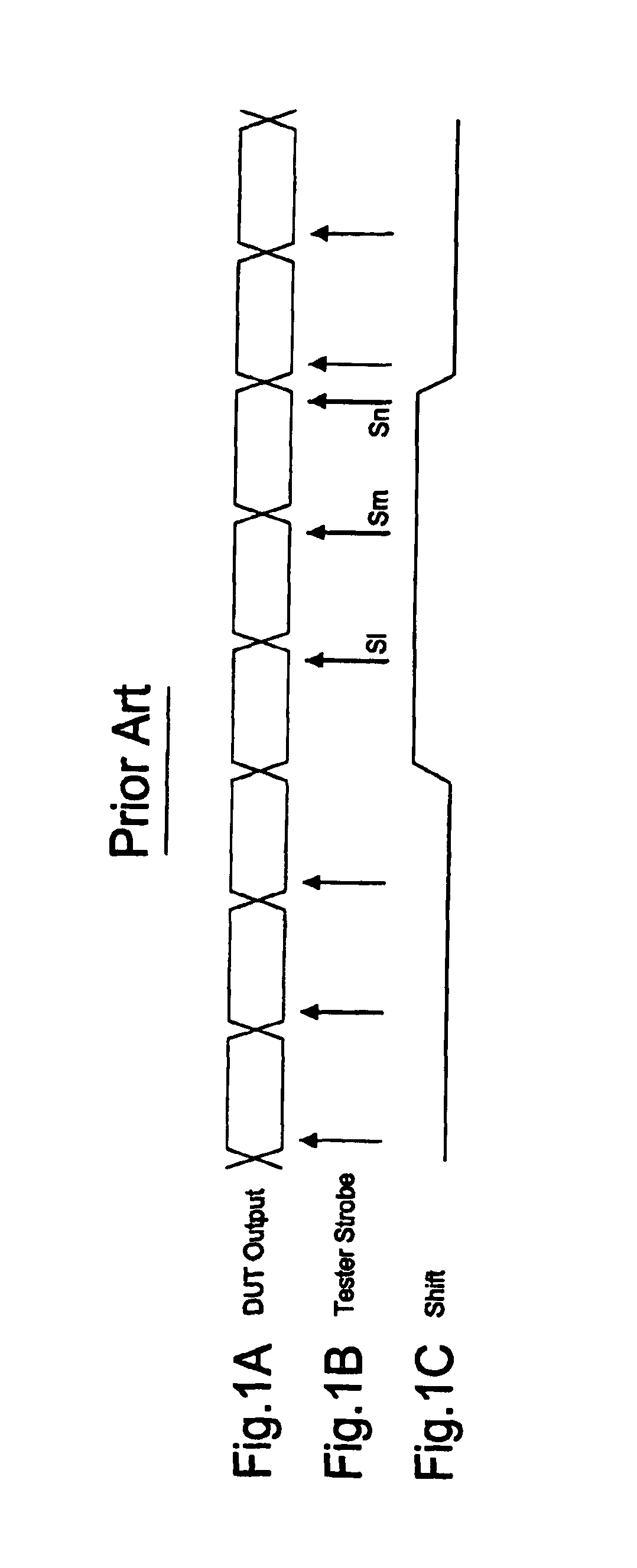
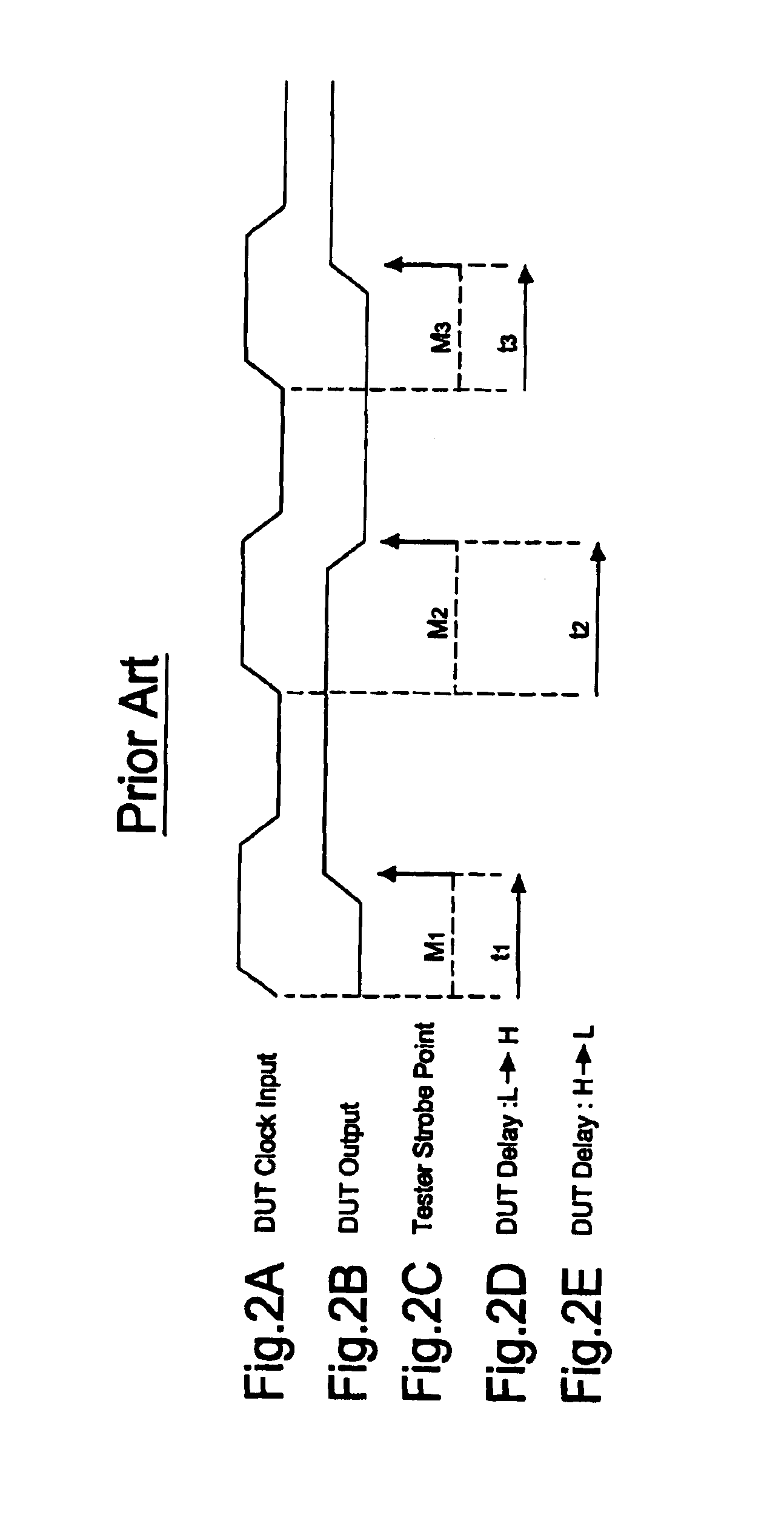
[0022]The time shift circuit and method of the present invention will be described in more detail with reference to the accompanying drawings. While the present invention will be described in conjunction with the functional test and AC parametric test of a semiconductor device, it will be understood that the present invention is not limited to such a specific application. For example, the present invention can also be applicable to a normal test when a timing of specific strobe or pattern edge is offset.
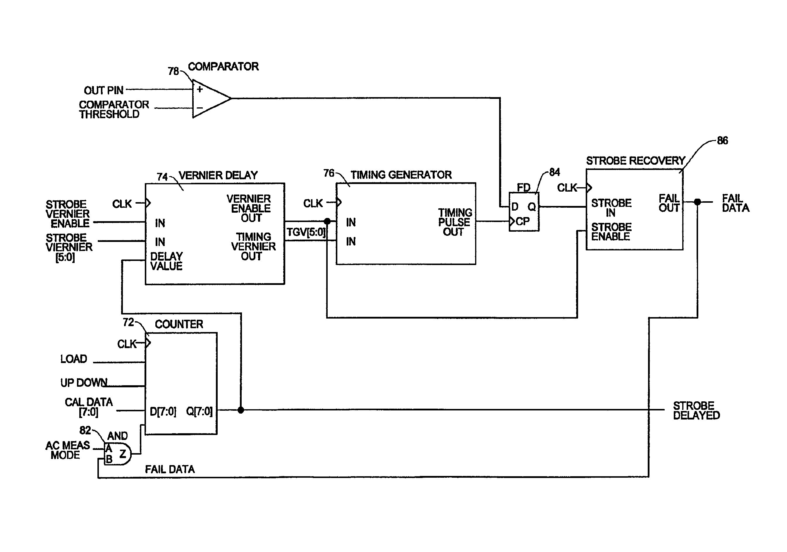
[0023]The basic structure of the time shift circuit of the present invention is shown in the block diagram of FIG. 3. The time shift circuit changes the times of desired timing edges on-the-fly. The time shift circuit includes a 2-to-1 multiplexer 12, a vernier delay unit 14, and a timing generator 16. In this arrangement, the vernier delay unit 14 provides timing data showing delay values to the timing generator 16 so that the timing generator produces timing edges with specified de...
PUM
 Abstract
Description
Claims
Application Information