Optical element, and manufacturing method thereof

a manufacturing method and optical element technology, applied in the field of optical elements, can solve the problems of insufficient study of swnt with respect to optical applications and formation of optically uniform films

Inactive Publication Date: 2005-08-30
NAT INST OF ADVANCED IND SCI & TECH
View PDF16 Cites 40 Cited by
  • Summary
  • Abstract
  • Description
  • Claims
  • Application Information

AI Technical Summary

Problems solved by technology

However, there is no specifically clear border therebetween.
However, the SWNT has not been sufficiently studied so far with respect to optical applications.
The primary reasons for the delay in optical application of the SWNT as compared with electric and electronic element applications may be due to the difficulty in obtaining a high purity sample of the SWNT required for optical evaluation, and the difficulty in forming an optically uniform film as the SWNT is hard to dissolve in solvents.

Method used


Image

  • Optical element, and manufacturing method thereof
  • Optical element, and manufacturing method thereof
  • Optical element, and manufacturing method thereof

Examples


Embodiment Construction

[0019]An optical element and a method for producing the same of the present invention will be described in detail below.

Details of Optical Element and Method for Producing the Same of the Present Invention

[0020]Carbon nanotubes include a single-wall carbon nanotube having a structure of a tube formed with a sheet of a hexagonal carbon lattice, and a multiwall carbon nanotube having a structure of a multi-layered (multi-walled) tube formed with plural carbon sheets mentioned above. The present invention employs single-wall carbon nanotubes that have a high saturable absorption function.

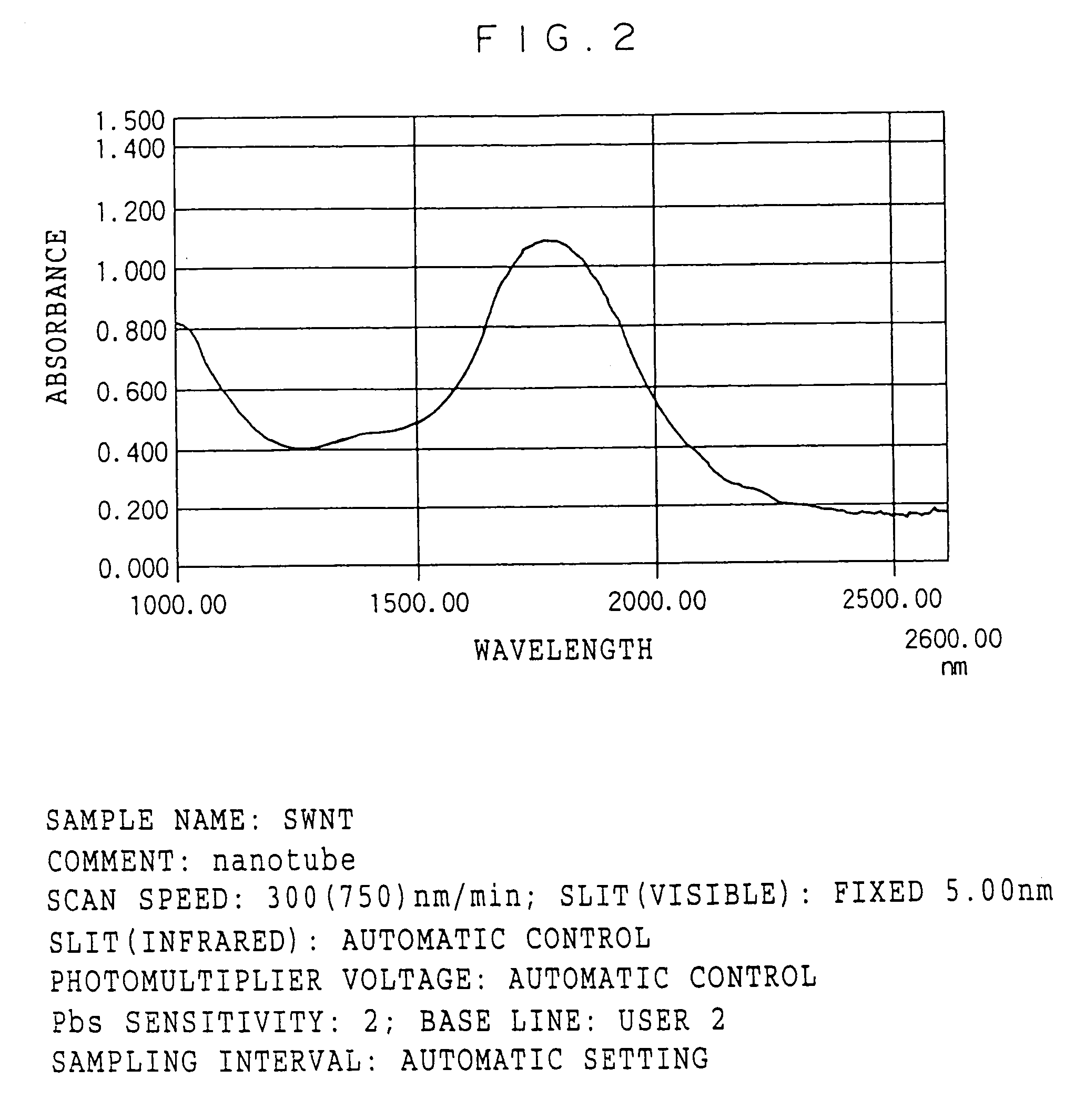
[0021]SWNTs having a diameter of 1.0 to 1.6 nm are preferably used. When the SWNTs having a diameter within the above range are used, the saturable absorption function is effectively exhibited.

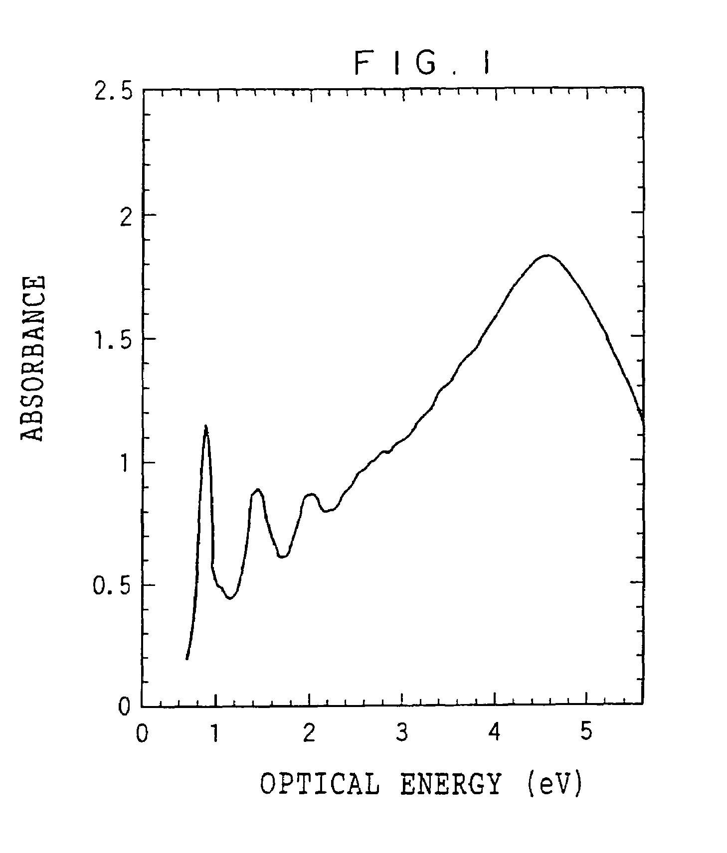
[0022]An optical element of the present invention utilizes optical absorption of quasi-one-dimensional exciton caused by interband transition, which originates in one-dimensional van Hove singularity of SWNTs in ...


PUM

PropertyMeasurementUnit
diameteraaaaaaaaaa
diameteraaaaaaaaaa
temperatureaaaaaaaaaa

Abstract

An optical element according to the present invention has a thin film, in which single-wall carbon nanotubes are laminated, and utilizes a saturable absorption function of the single-wall carbon nanotubes. Further, in a method for producing the optical element according to the present invention, the thin film is formed by spraying, to a body to be coated, a dispersion liquid prepared by dispersing the single-wall carbon nanotubes in a dispersion medium. Accordingly, a nonlinear optical element, which can operate in an optical communication wavelength region and which is extremely inexpensive and efficient, and a method for producing the optical element can be provided.

Description

TECHNICAL FIELD[0001]The present invention relates to an optical element (an optical device), which can control light in an optical communication wavelength region by utilizing a saturable absorption function of single-wall carbon nanotubes, and to a method for producing the optical element.BACKGROUND ART[0002]A carbon nanotube discovered recently is a tubular material, which is ideally formed with a sheet structure of a hexagonal carbon lattice (a graphene sheet) parallel to an axis of the tube. Further, the carbon nanotube may be a multi-layered tube formed with plural sheets mentioned above. In theory, the carbon nanotube is expected to exhibit a metallic or semiconducting property depending upon the connection type of the hexagonal carbon lattice and the diameter of the tube, and is expected as a future functional material.[0003]A material having a diameter of 1 μm or less, which is thinner than a carbon fiber, is commonly referred to as a carbon nanotube, and is thereby disting...

Claims


Application Information

Patent Timeline
Patent Type & Authority Patents(United States)
IPC IPC(8): G02B1/10G02F1/361G02F1/35G11B7/24G11B7/26B82Y10/00G02F1/01B82Y20/00B82Y30/00C01B32/152C01B32/158G02F1/355G11B7/257
CPCB82Y10/00G02B1/10G02F1/3523G02F1/361G11B7/24G11B7/243G11B7/257B82Y30/00Y10T428/21G02F1/3515G02F2203/26G11B7/2533G11B7/258G11B7/26G11B2007/24328Y10S977/742Y10S977/753
Inventor SAKAKIBARA, YOUICHITOKUMOTO, MADOKATATSUURA, SATOSHIACHIBA, YOHJIKATAURA, HIROMICHI
Owner NAT INST OF ADVANCED IND SCI & TECH
Why Eureka
Try Eureka