Phase-change memory cell and method of fabricating the phase-change memory cell

a phase-change memory and memory cell technology, applied in the field of phase-change memory cells and a method of fabricating the phase-change memory cells, can solve the problems of large-scale adoption of the phase-change mechanism for memory, the need to individually break-in each chalcogenide element for reproducible operation, etc., to achieve the effect of improving device yield and reliability

Inactive Publication Date: 2005-08-30
GLOBALFOUNDRIES INC
View PDF9 Cites 294 Cited by
  • Summary
  • Abstract
  • Description
  • Claims
  • Application Information

AI Technical Summary

Benefits of technology

[0007]In view of the foregoing and other problems, disadvantages, and drawbacks of the aforementioned conventional memory cells and methods of fabricating memory cells, it is a purpose of the exemplary aspects of the present invention to provide a memory cell and method of fabricating the memory cell which may improve device yield and reliability, and (e.g., at the same time) eliminate the need to individually break-in each phase-change element for reproducible operation.
[0008]The present invention also provides an efficient method for forming nanometer-scale pillar structures for a wide variety of materials including but not limited to the phase-change memory materials such as Ge2Sb2Te5 (or GST for short). The present invention includes a method which requires no subtractive etching of the phase-change materials (e.g., for the formation of the pillar structure), and hence can in principle be used for materials that are difficult to etch or for which no mature etching process has been developed, which could result in significant savings in development cost for the incorporation of new memory materials.
[0023]With its unique and novel features, the present invention provides a memory cell and method of fabricating the memory cell which may improve device yield and reliability, and (e.g., at the same time) eliminate the need to individually break-in each phase-change element for reproducible operation.

Problems solved by technology

In such cases often a “break-in” procedure is necessary for each chalcogenide cell to condition it such that it is stable for repeated current-induction of thermal cycling between the crystalline and amorphous states This procedure, plus the reliability problems associated with a large drive current passing through the chalcogenide for writing (large enough to cause a temperature swing of up to 600° C. locally involving current densities on the order of 106 A / cm2 through the chalcogenide), makes large-scale adoption of the phase-change mechanism for memory difficult.
These are two of the key issues facing the application of the chalcogenide-type of phase-change memories in mass-produced circuits.
Specifically, the issues include reliability associated with large current density through the chalcogenide element, and the need to individually break-in each chalcogenide element for reproducible operation.

Method used


Image

  • Phase-change memory cell and method of fabricating the phase-change memory cell
  • Phase-change memory cell and method of fabricating the phase-change memory cell
  • Phase-change memory cell and method of fabricating the phase-change memory cell

Examples


Embodiment Construction

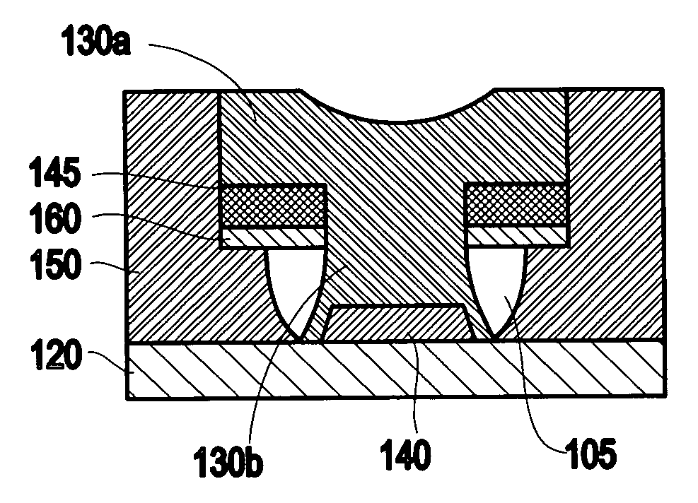
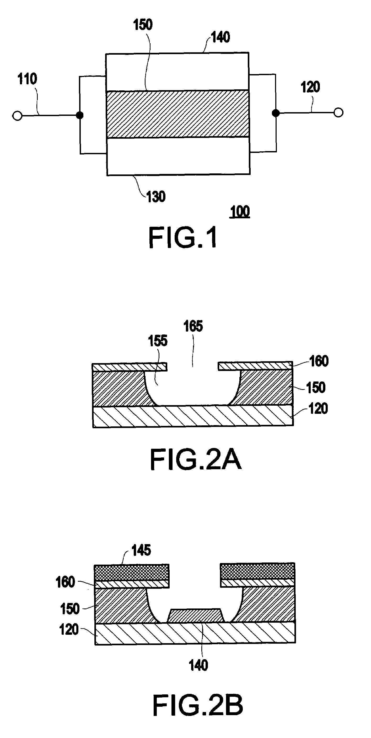
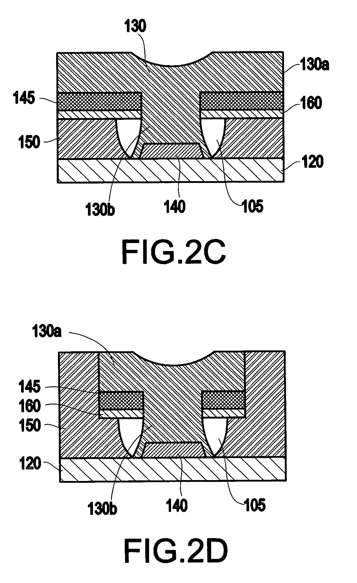
[0033]Referring now to the drawings, FIG. 1 illustrates a conceptual diagram of a memory cell 100 according to the present invention, and FIGS. 2A–2D, 3A–3D, 4A–4D, 5A–5D and 6A–6D illustrate exemplary embodiments of methods of fabricating the memory cell, according to the exemplary aspects of the present invention.

[0034]In a first exemplary aspect of the present invention (e.g., illustrated in FIG. 2D), a memory cell includes an insulating layer 150 formed on a first electrode layer 120, the insulating layer having an first opening 155, a stencil layer 160 formed on the insulating layer, and having a second opening 165 formed in an area of the first opening 155, a phase-change material layer 140 formed on a surface of the first electrode layer 120 in the first opening 155, and an electrically conductive layer 130 comprising a first portion 130a formed on the stencil layer 160 and defining a second electrode layer and a second portion 130b (e.g., a pillar-shaped structure) formed on...


PUM

PropertyMeasurementUnit
temperatureaaaaaaaaaa
temperature swingaaaaaaaaaa
areaaaaaaaaaaa

Abstract

A memory cell and method of fabricating the memory cell includes an insulating layer formed on a first electrode layer, the insulating layer having a first opening, a stencil layer formed on the insulating layer, and having a second opening formed in an area of the first opening, a phase-change material layer formed on a surface of the first electrode layer in the first opening, and an electrically conductive layer including a first portion formed on the stencil layer and defining a second electrode layer and a second portion formed on the phase-change material layer.

Description

BACKGROUND OF THE INVENTION[0001]1. Field of the Invention[0002]The present invention relates to a phase-change memory cell and a method of fabricating the memory cell and, more particularly, to a phase-change memory cell and a method of fabricating the memory cell in which a stencil layer is used to form a phase-change material layer.[0003]2. Description of the Related Art[0004]Nonvolatile memory elements based on the phase-change properties of the chalcogenide materials has a long history dating back to the '70s. Most known implementations of chalcogenide-based random access memory cells use the chalcogenide element both for read-out (based on its resistance change between the crystalline and amorphous state) and for write (based on Joule heating when current is passed through the chalcogenide).[0005]The resistivity of chalcogenide can vary over a very wide range from nearly insulating to fairly conducting. This could sometimes be useful during film deposition to create a differen...

Claims


Application Information

Patent Timeline
Patent Type & Authority Patents(United States)
IPC IPC(8): G11B7/24H01L29/06H01L29/02H01L29/47H01L27/085H01L29/812H01L27/095H01L29/66H01L29/40H01L39/00H01L45/00
CPCG11C13/0004G11C13/0069H01L45/06H01L45/1233H01L45/1286H01L45/144H01L45/1625H01L45/1666G11C2213/52H10N70/8613H10N70/231H10N70/026H10N70/061H10N70/8828H10N70/826
Inventor SUN, JONATHAN ZANHONGRAOUX, SIMONEWICHRAMASINGHE, HEMANTHA
Owner GLOBALFOUNDRIES INC
Why Eureka
Try Eureka